Download
1 / 6
60 likes | 141 Vues
Identification of an intrinsic difficulty in fabricating efficient power devices Sokrates T. Pantelides, Vanderbilt University, DMR 0907385.

E N D
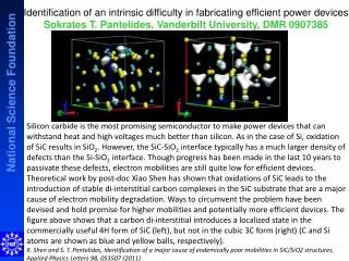
Identification of an intrinsic difficulty in fabricating efficient power devices SokratesT. Pantelides, Vanderbilt University, DMR 0907385 Silicon carbide is the most promising semiconductor to make power devices that can withstand heat and high voltages much better than silicon. As in the case of Si, oxidation of SiC results in SiO2. However, the SiC-SiO2 interface typically has a much larger density of defects than the Si-SiO2 interface. Though progress has been made in the last 10 years to passivate these defects, electron mobilities are still quite low for efficient devices. Theoretical work by post-doc Xiao Shen has shown that oxidations of SiC leads to the introduction of stable di-interstitial carbon complexes in the SiC substrate that are a major cause of electron mobility degradation. Ways to circumvent the problem have been devised and hold promise for higher mobilities and potentially more efficient devices. The figure above shows that a carbon di-interstitial introduces a localized state in the commercially useful 4H form of SiC (left), but not in the cubic 3C form (right) (C and Si atoms are shown as blue and yellow balls, respectively). X. Shen and S. T. Pantelides, Identification of a major cause of endemically poor mobilities in SiC/SiO2 structures, Applied Physics Letters 98, 053507 (2011)
Explanation of why sodium improves the properties of SiC-SiO2 interfaces for power devices SokratesT. Pantelides, Vanderbilt University, DMR 0907385 Silicon carbide is the most promising semiconductor to make power devices that can withstand heat and high voltages much better than silicon. As in the case of Si, oxidation of SiC results in SiO2. However, the SiC-SiO2 interface typically has a much larger density of defects than the Si-SiO2 interface. It has been shown by several investigators that introduction of sodium either during or after oxidation improves electron mobilities, as shown in the figure (left), but its role has been a mystery. Theoretical work by Blair Tuttle in conjunction with experimental data led to the conclusion that sodium atoms reside at the interface and create an “impurity band”, illustrated in the figure (right). This band enables relatively unimpeded flow of electrons in the SiC substrate. B. R. Tuttle, S. Dhar, S.-H. Ryu, X. Zhu, J. R. Williams, L. C. Feldman and S. T. Pantelides, “High electron mobility due to sodium ions in the gate oxide of SiC-metal-oxide-semiconductor field effect transistors”, Journal of Applied Physics, 109, 023702 (2011).
Phosphorous Passivation of the SiO2/4H-SiC Interface • Sokrates T. Pantelides, Vanderbilt University, DMR 0907385 Lower interface trap density (Dit) & higher effective mobility compared to industry standard nitrogen passivation process (NO) – both good. Penalty – Unstable FET threshold voltage for thermal SiO2 + P. Hard etching the thermal oxide & replacing it by a deposited oxide stabilizes Vth, but increases Dit. Underway: Controlled etching to remove near-interface P responsible for Vth instability while leaving P at the interface to keep Dit as low as possible. Preliminary results indicate that phosphorous in these two positions may be in different chemical configurations.
Interface Trap Density Following Nitridation with N2 Plasma is Comparable to Best Results Obtained Using Phosphorous To date with the N2 microwave plasma system, we have seen the interface trap density decrease with increasing N2 flow rate. The results shown were obtained using the maximum flow rate available to us ~ 3L/min. System upgrades over the next 3 months will increase our maximum flow rate to ~ 10L/min. • For similar annealing temperatures (~ 1175C) the interface trap density is lower using • an N2 microwave plasma compared to std NO. • Plasma Ditis comparable to phosphorous Dit, but w/o the threshold voltage instability • caused by near-interface phosphorous (in the form of phosphosilicate glass) in the oxide. Underway: MOSFET fabrication and characterization using the 8hr N2 plasma process.
Interface Trap Density Following Nitridation with N2 Plasma is Better than NO and Comparable to Best Results Obtained Using Phosphorous • Sokrates T. Pantelides, Vanderbilt University, DMR 0907385 To date with the N2 microwave plasma system, we have seen the interface trap density decrease with increasing N2 flow rate. The results shown were obtained using the maximum flow rate available to us ~ 3L/min. System upgrades over the next 3mo will increase our maximum flow rate to ~ 10L/min. The advantages of using a pure N2 microwave plasma instead of NO are the following. (1) We get more nitrogen to the interface for better trap passivation, so we should see higher mobility. (2) There is significantly less oxide growth during the plasma nitridation process compared to the industry standard NO process. This means that the combination of a low temperature (~ 600C) deposited oxide and plasma nitridation can be used to fabricate a “low carbon” MOSFET. By “low carbon”, we mean that the amount of carbon liberated during device fabrication is kept as low as possible and much, much lower than the amount liberated during thermal oxide growth followed by NO passivation. This is important because carbon that diffuses interstitially into the SiC near-interface channel region can subsequently form immobile carbon dimers that act as mobility limiting defects.
Workshop for High School Teachers • May 15, 2011 9 – 4 pm • Title: Energy and Materials • SokratesT. Pantelides, Vanderbilt University, DMR 0907385 Workshop was held at Behrend College and was attended by 9 teachers from around North West PA. The teachers received 8 hours credit toward their Act 48 continuing education requirement. Blair Tuttle (shown above with lantern) organized the workshop and Gerd Duscher was a presenter. The reviews of the workshop were overwhelmingly positive.