Advances in III-Sb Interfaces with High-k Oxides for Enhanced MOSFET Gate Stack Technology
This study explores the critical advancements in III-Sb interfaces when integrated with high-k oxides, focusing on the impact of threading dislocations and planar defects confined in a metamorphic superlattice buffer on GaAs substrates. Achievements include a significant reduction in dislocation density in GaSb, demonstrating maximum hole mobility of 1070 cm²/Vs at a 0.6% compressive strain. Two types of high-k oxides, Al2O3 and HfO2, were employed, showing interface trap densities near the conduction band of GaSb. This project included undergraduate and PhD student involvement and extensive community outreach.

Advances in III-Sb Interfaces with High-k Oxides for Enhanced MOSFET Gate Stack Technology
E N D
Presentation Transcript
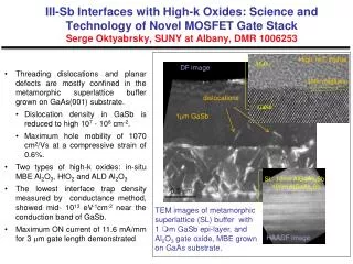
III-Sb Interfaces with High-k Oxides: Science and Technology of Novel MOSFET Gate StackSerge Oktyabrsky, SUNY at Albany, DMR 1006253 High-res. image DF image • Threading dislocations and planar defects are mostly confined in the metamorphic superlattice buffer grown on GaAs(001) substrate. • Dislocation density in GaSb is reduced to high 107 - 108 cm-2. • Maximum hole mobility of 1070 cm2/Vs at a compressive strain of 0.6%. • Two types of high-k oxides: in-situ MBE Al2O3, HfO2 and ALD Al2O3 • The lowest interface trap density measured by conductance method, showed mid- 1013 eV-1cm-2 near the conduction band of GaSb. • Maximum ON current of 11.6 mA/mm for 3 mm gate length demonstrated dislocations 1mm GaSb SL: 10nm AlGaAsxSb / 10nm AlGaAsySb TEM images of metamorphic superlattice (SL) buffer with 1 mm GaSbepi-layer, and Al2O3 gate oxide, MBE grown on GaAs substrate. HAADF image
Broader Impacts of the NSF Project Serge Oktyabrsky, SUNY at Albany, DMR 1006253 • CNSE 2011Summer Internship Programbrought 25 exceptional undergraduate students – including 17 NY State residents – to spend the summer exploring the emerging science of nanotechnology: One undergraduate student was on the 2011 summer internship under the NSF project (Fig.) • Three PhD students were directly involved in the project (one directly funded by NSF). • Presented at over 10 teleconferences, workshops and seminars to companies and organizations: Intel, Global Foundries, SRC, Marco; and conferences: 2011 MRS Spring Meeting (April 2011, San Francisco); International Conference on Molecular Beam Epitaxy, (August 2010, Berlin). • Community outreach activities were contributed by the students and staff supported by this project: 'Nanovember,' CNSE Community Day, ‘Nanocarrier days’ (more details at http://cnse.albany.edu/Outreach/CNSEOutreachReport.aspx). Rocco Cammarere (left), undergraduate student from Clarkson University, during the 2011 Undergraduate Internship Program Poster Presentation Session, presenting his poster “Detection of MOSFET Interface Traps Using Self Consistent Solver and Gated Hall Measurements”