Download
1 / 37
390 likes | 451 Vues
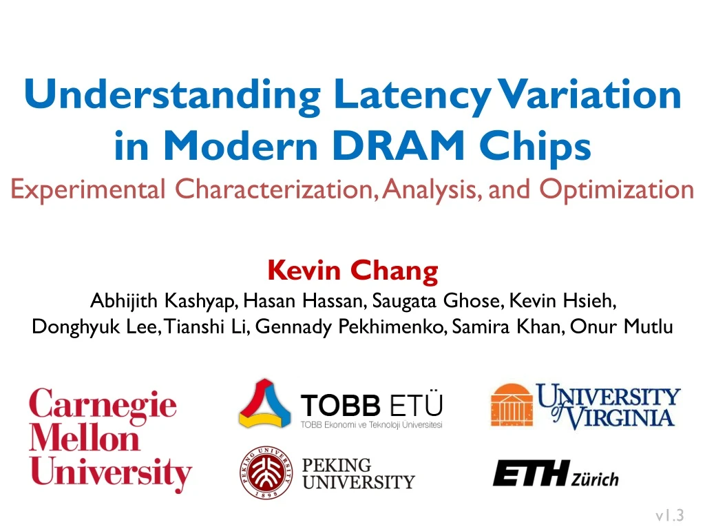
Understanding Latency Variation in Modern DRAM Chips Experimental Characterization, Analysis, and Optimization. Kevin Chang Abhijith Kashyap , Hasan Hassan, Saugata Ghose , Kevin Hsieh, Donghyuk Lee, Tianshi Li, Gennady Pekhimenko , Samira Khan, Onur Mutlu. v1.3.

E N D
Understanding Latency Variation in Modern DRAM ChipsExperimental Characterization, Analysis, and Optimization Kevin Chang AbhijithKashyap, Hasan Hassan, SaugataGhose, Kevin Hsieh, Donghyuk Lee, Tianshi Li, Gennady Pekhimenko,Samira Khan, OnurMutlu v1.3
Main Memory Latency Lags Behind 64x 16x 1.2x Long DRAM latency → performance bottleneck In-memory DB, Spark, JVM, … [Clapp+ (Intel), IISWC’15] Google warehouse-scale workloads [Kanev+ (Google), ISCA’15]
Why is Latency High? • DRAM latency: Delay as specified in DRAM standards • Doesn’t reflect true DRAM device latency • Imperfect manufacturing process → latency variation • High standard latency chosen to increase yield Low High Standard Latency DRAM A DRAM B DRAM C ManufacturingVariation DRAMLatency
Goals 1 1 Understand and characterize latency variation in modern DRAM chips 2 2Develop a mechanism that exploits latency variation to reduce DRAM latency
Outline • Motivation and Goals • DRAM Background • Experimental Methodology • Characterization Results • Mechanism: Flexible-Latency DRAM • Conclusion
High-Level DRAM Organization DRAM chip DRAM Channel DIMM (Dual in-line memory module)
DRAM Chip Internals … DRAMCell … … Row Buffer 8KB (128 cache lines)
DRAM Operations ACTIVATE: Store the row intothe row buffer 1 1 1 1 1 READ: Select the target cache line and drive to CPU 2 3 PRECHARGE: Prepare the array for a new ACTIVATE to CPU
DRAM Timing Parameters 2 Precharge latency: tRP(13ns / 50 cycles) Command Data Cache line (64B) Duration Next ACT ACTIVATE READ PRECHARGE 1 Activation latency: tRCD(13ns / 50 cycles) 1 1 1 1
DRAM Latency Variation Imperfect manufacturing process→ latency variation Low High DRAM B DRAM A DRAM C Slowcells DRAMLatency
Experimental Questions Imperfect manufacturing process→ latency variation Can we show latency variation in these parameters? How large is latency variation in modern DRAM chips? Can we identify the properties of slow cells with long latency? Can we isolate slow cells to make DRAM faster?
Experimental Methodology • Tool that enables us to freely issue DRAM commands • Existing systems: Commands are generated and controlled by HW • Custom FPGA-based infrastructure PCIe DDR3 PC DIMM FPGA Generate command sequence C++ programs to specifycommands
Experiments • Swept each timing parameter to read data • Time step of 2.5ns (FPGA cycle time) • Quantifiedtiming errors: bit flips when using reduced latency • Tested 240 DDR3 DRAM chips from three vendors • 30 DIMMs • Manufacturing dates: 2011 – 2013 • Capacity: 1GB • Ambient temperature: 20oC
Outline • Motivation and Goals • DRAM Background • Experimental Methodology • Characterization Results • Activation latency • Precharge latency • Mechanism: Flexible-Latency DRAM • Conclusion
Activation Latency: Key Observation Observation: ACT errors are isolated in the cells read in the first cache line Command 1 1 1 1 Not fullyactivated Actual ACT Time tRCD 1 1 1 ? ? Row Buffer Second read w/ sufficient activation time First read after ACT 0 1 X READ ACTIVATE READ
Variation in Activation Errors No ACT Errors Results from 7500 rounds over 240 chips Many errors Very few errors Max Rife w/ errors 13.1ns standard Min Quartiles Modern DRAM chips exhibit significant variation in activation latency Different characteristics across DIMMs
Spatial Locality of Activation Errors One DIMM @ tRCD=7.5ns Activation errors are concentrated at certain columns of cells
Strong Pattern Dependence DIMM A DIMM B DIMM C > 4 orders of magnitude Row buffer design is biased towards 1 over 0 [Lim+, ISSCC’12] Activation errors have a strong dependenceon the stored data patterns
Precharge Latency: Key Observation Observation: PRE errors occur in multiple cache lines in the row activated after a precharge Command 1 1 1 1 Not fullyprecharged Actual PRE Time tRP 0 0 0 0 1 0 1 1 0 1 Row Buffer Incorrectly sensed data PRECHARGE ACTIVATE
Variation in Precharge Errors No PRE Errors Results from 4000 rounds over 240 chips Rife w/ errors Many errors Few errors 13.1ns standard Different characteristics across DIMMs Modern DRAM chips exhibit significant variation in precharge latency
Spatial Locality of Precharge Errors One DIMM @ tRP=7.5ns Precharge errors are concentrated at certain rows of cells
Outline • Motivation and Goals • DRAM Background • Experimental Methodology • Characterization Results • Mechanism: Flexible-Latency DRAM • Conclusion
Mechanism to Reduce DRAM Latency • Observations • DRAM timing errors are concentrated on certain regions • All cells operate without errors at 10ns tRCD and tRP • Flexible-LatencY(FLY) DRAM • A software-transparent design that reduces latency • Key idea: 1) Divide memory into regions of different latencies 2) Memory controller: Uselower latency for regions without slow cells;higher latency for other regions
FLY-DRAM Evaluation Methodology • Cycle-level simulator: Ramulator[CAL’15]https://github.com/CMU-SAFARI/ramulator • 8-core system with DDR3 memory • Benchmarks: SPEC2006, TPC, STREAM, random • 40 8-core workloads • Performance metric: Weighted Speedup (WS)
FLY-DRAM Configurations tRCD 99% 93% 12% Profiles of 3 real DIMMs tRP 99% 74% 13%
Results 19.7% 19.5% 17.6% 13.3% FLY-DRAM improves performance by exploiting latency variation in DRAM
Other Results in the Paper • Error-correcting codes (ECC) • Effective at correcting activation errors • Restoration latency • Significant margin to complete without errors • Effect of temperature • Difference is not statistically significant to draw conclusion
Conclusion • First to experimentally demonstrate and analyze latency variation behavior within real DRAM chips • Showacross 240 DRAM chips that: • All cellswork below standard latency • Some regions of cells work even faster, but slow cells in other regions start to fail • Error rate is data-dependent • FLY-DRAM reduces latency by using low latency for regions without slow cells and high latency for others • 13%/17%/19% speedup based on profiles of 3 real DIMMs https://github.com/CMU-SAFARI/DRAM-Latency-Variation-Study
Understanding Latency Variation in Modern DRAM ChipsExperimental Characterization, Analysis, and Optimization Kevin Chang AbhijithKashyap, Hasan Hassan, SaugataGhose, Kevin Hsieh, Donghyuk Lee, Tianshi Li, Gennady Pekhimenko,Samira Khan, OnurMutlu
Infrastructure TemperatureController FPGA DIMM Heater