Download
1 / 2
20 likes | 225 Vues
Sn-based Group-IV Semiconductors: A new Platform for Opto- and Microelectronics on Si John Kouvetakis, Arizona State University, DMR-0221993.

E N D
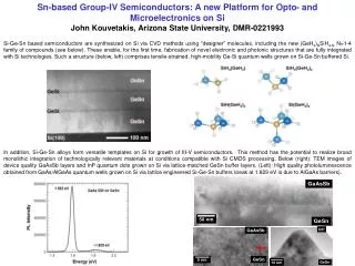
Sn-based Group-IV Semiconductors: A new Platform for Opto- and Microelectronics on Si John Kouvetakis, Arizona State University, DMR-0221993 Si-Ge-Sn based semiconductors are synthesized on Si via CVD methods using “designer” molecules, including the new (GeH3)NSiH4-N N=1-4 family of compounds (see below). These enable, for the first time, fabrication of novel electronic and photonic structures that are fully integrated with Si technologies. Such a structure (below, left) comprises tensile-strained, high-mobility Ge-Si quantum wells grown on Si-Ge-Sn buffered Si. In addition, Si-Ge-Sn alloys form versatile templates on Si for growth of III-V semiconductors. This method has the potential to realize broad monolithic integration of technologically relevant materials at conditions compatible with Si CMOS processing. Below (right):TEM images of device quality GaAsSb layers and InP quantum dots grown on Si via lattice-matched GeSn buffer layers. (Left): High quality photoluminescence obtained from GaAs/AlGaAs quantum wells grown on Si via lattice engineered Si-Ge-Sn buffers (peak at 1.829 eV is due to AlGaAs barriers).
Sn-based Group-IV Semiconductors: A new Platform for Opto- and Microelectronics on Si John Kouvetakis, Arizona State University, DMR-0221993 Human Resources: Graduate students Candi Cook, Rahul Trivedi, Radek Roucka, Tito Garza, Lily An, and Jesse Tice were funded in part by the grant during the academic year 2004-2005. Roucka received his Ph.D. in December 2004 and Trivedi defended his M.S. thesis in May 2005. Technology Transfer and Industrial Outreach • We have partnered with Voltaix Corporation (a leading manufacturer of semiconductor gas products) through a technology licensing agreement to commercialize innovations developed using the grant. These include scaleable industrial syntheses of new families of hydride compounds and their use to deposit materials for applications in advanced substrates for strained Si channels, CMOS-integrated MEMS, solar cells and silicon based nanoscale photonics. The project will demonstrate proof of concept applications in leading technologies. Voltaix has licensed two patents stemming from our NSF funded research. • We have partnered with the Photonics Technology Lab at Intel Corporation in Santa Clara to develop group IV optical devices based on Si-Ge-Sn quantum wells. This work is supported with a 3-year grant provided by Intel Corporation. • 3. Recent NSF supported graduates of our group, John Tolle and Radek Roucka, are forming a spin off company with SBIR and STTR grants/contracts to develop specialized components of IR detection and imaging systems for military applications. • 4. Work developed under this grant has led to a small business technology transfer award (STTR) provided by AFOSR in partnership with QuanTerra Corporation (Scottsdale Arizona) to develop a Si-based laser.