Download
1 / 32
330 likes | 364 Vues
Learn about the operation of full bridge converters below and above resonance, focusing on zero-current/voltage switching methods and load-dependent properties. Topics include switching sequences, inverter design objectives, and transistor currents. Dive into practical examples and analysis for better understanding and efficient design.

E N D
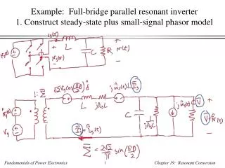
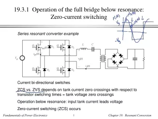
19.3.1 Operation of the full bridge below resonance: Zero-current switching Series resonant converter example Current bi-directional switches ZCS vs. ZVS depends on tank current zero crossings with respect to transistor switching times = tank voltage zero crossings Operation below resonance: input tank current leads voltage Zero-current switching (ZCS) occurs
Tank input impedance Operation below resonance: tank input impedance Zi is dominated by tank capacitor. Zi is negative, and tank input current leads tank input voltage. Zero crossing of the tank input current waveform is(t) occurs before the zero crossing of the voltage vs(t) – before switch transitions
Switch network waveforms, below resonanceZero-current switching Conduction sequence: Q1–D1–Q2–D2 Tank current is negative at the end of each half interval – antiparallel diodes conduct after their respective switches Q1 is turned off during D1 conduction interval, without loss
Classical but misleading example: Transistor switchingwith clamped inductive load (4.3.1) Buck converter example transistor turn-off transition Loss:
ZCS turn-on transition: hard switching Q1 turns on while D2 is conducting. Stored charge of D2 and of semiconductor output capacitances must be removed. Transistor turn-on transition is identical to hard-switched PWM, and switching loss occurs.
19.3.2 Operation of the full bridge above resonance: Zero-voltage switching Series resonant converter example Operation above resonance: input tank current lags voltage Zero-voltage switching (ZVS) occurs
Tank input impedance Operation above resonance: tank input impedance Zi is dominated by tank inductor. Zi is positive, and tank input current lags tank input voltage. Zero crossing of the tank input current waveform is(t) occurs after the zero crossing of the voltage vs(t) – after switch transitions
Switch network waveforms, above resonanceZero-voltage switching Conduction sequence: D1–Q1–D2–Q2 Tank current is negative at the beginning of each half-interval – antiparallel diodes conduct before their respective switches Q1 is turned on during D1 conduction interval, without loss – D2 already off!
ZVS turn-off transition: hard switching? When Q1 turns off, D2 must begin conducting. Voltage across Q1 must increase to Vg. Transistor turn-off transition is identical to hard-switched PWM. Switching loss mayoccur… but….
Classical but misleading example: Transistor switchingwith clamped inductive load (4.3.1) Buck converter example transistor turn-off transition Loss:
Soft switching at the ZVS turn-off transition • Introduce small capacitors Cleg across each device (or use device output capacitances). • Introduce delay between turn-off of Q1 and turn-on of Q2. Tank current is(t) charges and discharges Cleg. Turn-off transition becomes lossless. During commutation interval, no devices conduct. So zero-voltage switching exhibits low switching loss: losses due to diode stored charge and device output capacitances are eliminated. Also get reduction in EMI.
Chapter 19Resonant Conversion • Introduction • 19.1 Sinusoidal analysis of resonant converters • 19.2 Examples • Series resonant converter • Parallel resonant converter • 19.3 Soft switching • Zero current switching • Zero voltage switching • 19.4 Load-dependent properties of resonant converters • 19.5 Exact characteristics of the series and parallel resonant converters
19.4 Load-dependent propertiesof resonant converters • Resonant inverter design objectives: • 1. Operate with a specified load characteristic and range of operating points • With a nonlinear load, must properly match inverter output characteristic to load characteristic • 2. Obtain zero-voltage switching or zero-current switching • Preferably, obtain these properties at all loads • Could allow ZVS property to be lost at light load, if necessary • 3. Minimize transistor currents and conduction losses • To obtain good efficiency at light load, the transistor current should scale proportionally to load current (in resonant converters, it often doesn’t!)
Topics of DiscussionSection 19.4 • Inverter output i-v characteristics • Two theorems • Dependence of transistor current on load current • Dependence of zero-voltage/zero-current switching on load resistance • Simple, intuitive frequency-domain approach to design of resonant converter • Example • Analysis valid for resonant inverters with resistive loads as well as resonant converters operating in CCM
CCM PWM vs. resonant inverter output characteristics • CCM PWM • Low output impedance – neglecting losses, output voltage function of duty cycle only, not of load • Steady-state IV curve looks like voltage source • Resonant inverter (or converter operating in CCM) • Higher output impedance – output voltage strong function of both control input and load current (load resistance) • What does steady-state IV curve look like? (i.e. how does || v || depend on || i ||?)
Analysis of inverter output characteristics – simplifying assumptions • Load is resistive • Load does not change resonant frequency • Can include any reactive components in tank • Resonant network is purely reactive (neglect losses)
Thevenin equivalent of tank network output port Voltage divider Sinusoidal steady-state
Inverter output characteristics • Let H be the open-circuit (R→) transfer function: and let Zo0 be the output impedance (with vi→short-circuit). Then, This result can be rearranged to obtain The output voltage magnitude is: Hence, at a given frequency, the output characteristic (i.e., the relation between ||vo|| and ||io||) of any resonant inverter of this class is elliptical. with
with Inverter output characteristics • General resonant inverter output characteristics are elliptical, of the form This result is valid provided that (i) the resonant network is purely reactive, and (ii) the load is purely resistive.
Matching ellipseto application requirements Electronic ballast Electrosurgical generator
Example of gas discharge lamp ignition and steady-state operation from CoPEC research LCC resonant inverter Vg = 300 V Iref = 5 A
Example of repeated lamp ignition attempts with overvoltage protection LCC resonant inverter Vg = 300 V Iref = 5 A Overvoltage protection at 3500 V
19.4 Load-dependent propertiesof resonant converters • Resonant inverter design objectives: • 1. Operate with a specified load characteristic and range of operating points • With a nonlinear load, must properly match inverter output characteristic to load characteristic • 2. Obtain zero-voltage switching or zero-current switching • Preferably, obtain these properties at all loads • Could allow ZVS property to be lost at light load, if necessary • 3. Minimize transistor currents and conduction losses • To obtain good efficiency at light load, the transistor current should scale proportionally to load current (in resonant converters, it often doesn’t!)
ZN and ZD ZD is equal to the tank output impedance under the condition that the tank input source vs1 is open-circuited. ZD = Zo ZN is equal to the tank output impedance under the condition that the tank input source vs1 is short-circuited. ZN = Zo0
Magnitude of the tank input impedance If the tank network is purely reactive, then each of its impedances and transfer functions have zero real parts, and the tank input and output impedances are imaginary quantities. Hence, we can express the input impedance magnitude as follows:
A Theorem relating transistor current variations to load resistance R • Theorem 1: If the tank network is purely reactive, then its input impedance || Zi || is a monotonic function of the load resistance R. • So as the load resistance R varies from 0 to , the resonant network input impedance || Zi || varies monotonically from the short-circuit value|| Zi0 || to the open-circuit value || Zi ||. • The impedances || Zi || and || Zi0 || are easy to construct. • If you want to minimize the circulating tank currents at light load, maximize || Zi ||. • Note: for many inverters, || Zi || < || Zi0 || ! The no-load transistor current is therefore greater than the short-circuit transistor current.
Proof of Theorem 1 • Differentiate: • Previously shown: • Derivative has roots at: So the resonant network input impedance is a monotonic function of R, over the range 0 < R < . In the special case || Zi0 ||=|| Zi||,|| Zi || is independent of R.