Download
1 / 10
100 likes | 128 Vues
Learn how to design a lead/lag network for system stability by manipulating transfer functions and dissecting the effects of first-order lead/lag terms. Understand how to adjust phase shift and gain considerations to improve system performance. Discover practical applications and examples for buck converter control and loop compensation.

E N D
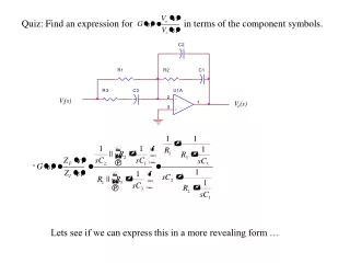
Quiz: Find an expression for in terms of the component symbols. Vi(s) Vo(s) - Lets see if we can express this in a more revealing form …
Manipulate transfer function to rational fraction form . . . This represents a second order lead/lag network with integration. The following symbolic associations apply: It is often desirable to make the zero frequencies the same, and the pole frequencies the same: Then . . Two identical first order lead/lag terms Linear gain Integration
Dissecting the effects of a first order lead/lag term : The phase at any frequency (s = jw) is: Maximum phase shift occurs when the derivative is zero: The maximum phase shift, given wz and wp (or the ratio wp / wz) can be expressed:
Dissecting the effects of a first order lead/lag term (cont) : If the desired maximum phase shift is specified, we can determine the required ratio wp / wz : Gain Considerations: The magnitude of the transfer function (gain) of the standard form first order lead/lag network at any frequency w is: The gain magnitude at the frequency of maximum phase shift is determined when :
Summary: A lead/lag network is used to compensate feedback loops that exhibit too much phase lag (approaching or exceeding 180o) at frequencies where the magnitude of the loop gain is greater than 0 dB. The strategy is to identify a critical frequency where the phase lag is to be adjusted, and then to adjust the phase by a specified amount in order to meet some desired phase margin specification. Since phase margin is defined at the crossover (0 dB) frequency of the open loop transfer function, it is common practice to choose a desired crossover frequency , wA, (usually, but not necessarily, near the low-pass break frequency of the uncompensated loop gain) as the critical frequency for establishing how much phase adjustment the lead/lag compensation should provide. Since the gain magnitude of the compensating network (kc) can usually be set independently, the overall loop gain and crossover frequency can also be determined by our choice of kc . The relations developed above allow the designer to choose the break frequencies (wz and wp) of the lead/lag network in order to provide the required phase adjustment, YA at a specific frequency, wA:
Application: Buck Converter Control VIN GPS(s) (Linearized Power Stage Model) Loop Compensation VREF GC(s) ( ) GPWM + - Load kFB We examine stability of the closed loop system by determining the gain and phase margins of the Open Loop Transfer Function: From example 4.1: From example 4.2, for the Buck Converter (eq 4.15): 1.8 v DT v +(t) VB
Digression: Relating Closed Loop behavior to Open Loop transfer function (“Loop Gain”). GOL(s) (Controller) + - GOL(s) usually exhibits a low pass characteristic with considerable gain at low frequencies. As a result, at low frequencies when | GOL(s) | >> 1,GCL(s) ~ 1, and the output follows the input variations very closely. At higher frequencies when | GOL(s) | << 1,GCL(s) ~ GOL(s), and the high frequency variations in the input appear at the output highly attenuated. To say it another way, changes to the input (or other disturbances) that occur at high frequencies do not materially affect the output. In between these two frequency ranges, when | GOL(s) | ~ 1, the response of the system transitions from following changes in the input, to not following changes in the input. This is the critical range where gain and phase margin are determined. The frequency wc, where |GOL (jwc)| = 1 (0 dB) is called the crossover frequency, and the phase lag must be less than p radians below wc or the system will exhibit instability. Referring to the Bode plot for the Power Stage, we can conclude that a simple controller exhibiting only linear gain will be stable, but will also exhibit a steady state output error. Example 4.3 invokes the requirement that there be zero steady state output error, which implies an integrator in the controller. An integrator always introduces p/2 phase lag at all frequencies, and the additional phase lag will cause a total phase lag Y > p when |GOL (s)| > 1. BAD JUJU.
Example 4.3 • Zero Steady State Error • Phase Margin of p/3 • kFB= 0.2 • Crossover frequency greater than low pass corner of LC filter. Design the Compensator: The unknown part of the controller transfer function must introduce additional leading phase in the vicinity of the resonance frequency of the LC filter where its phase lag is greatest. Choose loop crossover frequency to be 1000 hz. This just happens to be where the Power Stage phase lag is maximum ~ 138o . With the additional 90o lag of the integrator, this will give a total phase lag of 228o. In order to have a phase margin of 60o, our compensator must introduce 108o of phase lead at the crossover frequency. Since a first order lead/lag compensator cannot provide even 90o of lead, we must use a second order lead/lag . . . . Low pass corner (resonance) of LC filter, ~ 600 hz = 17.1
. . . Which just happens to be consistent with the transfer function of the previously analyzed circuit. Who’d have guessed? The second order network must provide 108o of phase lead at fA = 1000 hz, which is twice the phase shift of a first order network. Therefore, the maximum phase shift, YA , of each of the first order networks must be 54o. At 1000 hz, (w = wA = 2000p), the compensated loop gain should be equal to 1 (0 dB). Recalling that the magnitude of the first order lead/ lag term when w = wA is
We can now use the cookbook formulae from the circuit analysis to solve for component values. We have five equations in six unknowns. If we choose R1 to be 10,000 ohms, we get the following solution: R1 = 10,000 W R2 = 1910 W R3 = 1180 W C1 = 0.256 mF C2 = 0.0302 mF C3 = 0.0438 mF Multiplying all resistor values and dividing all capacitor values by any scaling constant will yield valid solutions.