Download
1 / 35
370 likes | 474 Vues
Explore CMP process model development and integration with CAD. Enhance design for manufacturing with validation feedback and supply chain constraints, maximizing impact, flexibility, and quality while minimizing costs and environmental impacts.

E N D
CMP Modeling as Part of Design for Manufacturing David Dornfeld Will C. Hall Professor of Engineering Laboratory for Manufacturing and Sustainability Department of Mechanical Engineering University of California Berkeley CA 94720-1740 http://lmas.berkeley.edu
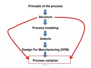
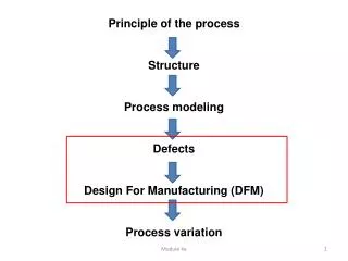
Outline • Modeling objectives and perspective • CMP process model development • Short review • Towards design for manufacturing (DFM)
Hardware driven Software driven Levels of Flexibility - Design to Manufacturing
Functional Model Feedback (validation) Prototype based on model Integration with CAD Include “islands of automation” and existing models) Feedback (validation) Feedback (validation) Feedback (validation) Include supply chain with constraints (e.g. “quality gates” ) Extend to “social impact” constraints (green, sustainability, health, safety, etc.) Feedback (validation) Feedback (validation) Modeling Roadmap for maximum impact Minimum cost/CoO Maximum production Maximum flexibility Maximum quality Minimum environmental & social impact Broadest integration * * * Through software
Is there need for this? Design Manf’g Design Manf’g
Design + Manf’g Manf’g + Design What you see depends on where you are standing! Source: Y. Granik, Mentor Graphics
What’s your world view? Process Process Process Design Design Design
Components of Chemical Mechanical Planarization Mechanical Phenomena Chemical Phenomena Interfacial and Colloid Phenomena
Mechanical particle forces Particle enhanced chemistry Material Removal Active Abrasives Pores, Walls Grooves Pad Tool mechanics, Load, Speed Chemical Reactions Mechanism Layout wafer dies critical features Scale/size nm mm µm Scale Issues in CMP From E. Hwang, 2004
Better planarization efficiency Better control of WIWNU Smaller WIDNU Small dishing & erosion Reducing scratch defects Reducing ‘Fang’ Reducing slurry usage Uniform pad performance thru it’s lifetime Longer pad life time Ultra low-k integration model E-CMP design goal Pad development An overview of CMP research in Berkeley Cu CMP Bulk Cu CMP Barrier polishing W CMP Oxide CMP Poly-Si CMP Bulk Cu slurry Barrier slurry W slurry Oxide slurry Poly-Si slurry Abrasive type, size and concentration Dornfeld Doyle Talbot [oxidizer], [complexing agent], [corrosion inhibitor], pH … Chemical reactions Mechanical material removal mechanism in abrasive scale Pad asperity density/shape Pad mechanical properties in abrasive scale Physical models of material removal mechanism in abrasive scale Pattern Topography MIT model Models of WIDNU Pad properties in die scale Slurry supply/ flow pattern in die scale Pad design Wafer scale pressure NU Models of WIWNU Wafer scale velocity profile Fabrication Fabrication technique Wafer bending with zone pressures Slurry supply/ flow pattern in wafer scale Test Pad groove
Choi (FLCC) MRR = CMP Modeling History in SFR/FLCC* now before SFR/FLCC DfM/MfD Preston’s Eqn. MRR = CPV Combined eqn. R=CM/(C+M) Luo (SFR) MRR= N Vol Tripathi (FLCC) Tribo-electro-chemical model Computational efficiency Flexible in scale Process links Interfacial/colloidal effects * According to Dornfeld
Interactions between Input Variables Four Interactions:Wafer-Pad Interaction; Pad-Abrasive Interaction; Wafer-Slurry Chemical Interaction; Wafer-Abrasive Interaction Velocity V Vol Chemically Influenced Wafer Surface Wafer Abrasive particles on Contact area with number N Abrasive particles in Fluid(All inactive) Pad asperity Polishing pad Active abrasives on Contact area Source: J. Luo and D. Dornfeld, IEEE Trans: Semiconductor Manufacturing, 2001
Stage 1 Stage 2 Df S=S0 Stage 3 Hcu0 S1=Df1 H= Hstage1 H=Hcu0+Hox0 1 2 3 Erosion e Dishing d Hox0 Pad Materials/Shape Effects Dishing and erosion Linear Viscoelastic Pad Pad/wafer contact modes in damascene polishing
Effect of Pattern Density - Planarization Length (PL) High-density region Global step Low-density region ILD Metal lines Planarization Length
Effective pattern density a=320um < Test pattern > a=640um a=1280um < Post CMP film thickness prediction at die-scale > < Effective density map > Modeling of pattern density effects in CMP Planarization length (window size) effect on “Up area”
F_tent > F_die ? F_tent < F_die ? No No Yes Yes ++Z_pad --Z_pad Z_pad Feature level interaction between pad asperities and pattern topography PAD Z(x,y) Z_pad Reference height (z=0) dz Z(x,y) z Z_pad
Asperity Height (µm) Probability Density (µm-1) a b active asperities (source : A.Scott Lawing, NCCAVS, CMPUG 5/5/2004) Characterization of Pad Surface
Model for the simulation fitting parameter accounting for chemical reactions, abrasive size distribution etc. abrasive particle size asperity radius pad/film properties polishing speed pad asperity height distribution New model pattern density effect Mean distance between asperities hardness of material polished
Modeling Overview Chip Layout Pattern density Line width Line space CMP Input Thickness HDP-CVD Deposition Model CMP model Nitride thinning Evolution
Planarization, Uniformity, Defects Incoming topography Adding the electro-chemical effects • Develop a transient tribo-electro-chemical model for material removal during copper CMP • Experimentally investigate different components of the model • Using above model develop a framework for pattern dependency effects. Slurry chemistry (pH, conc. of oxidizer, inhibitor & complexing agent) CMP Model 1. Passivation Kinetics 2. Mechanical Properties of Passive Film 3. Abrasive-copper Interaction Frequency & Force Pad properties layers’ hardness, structure Removal Rate (RR) Abrasive Type, size & conc. Polishing conditions (pressure P, velocity V) Polished material
Application: Polishing induced stress Pressure concentrated locally (about 300 psi) Risk of cracking in the sub layers
FEM Analysis: Model COPPER Layer E = 129.8 GPa ; α = 0.34 TANTALUM Layer E = 185.7 GPa ; α = 0.34 LOW-K Layer E = 5 – 20 GPa ; α = 0.25 BOUNDARY CONDITIONS: - Fixed at the bottom - Periodic Boundary Conditions (symmetry) LOADS: - Downward Constant Pressure – 2psi - Horizontal Shear (friction) stress – 0.7psi
Step1 Step2 Step3 Step3 FEM Analysis in CMP Von Mises stresses Low-k: E = 5GPa Low-k: E = 20GPa
Present methods treat CMP process as a black box; are blind to process & consumable parameters Need detailed process understanding For modeling pattern evolution accurately Present methods do not predict small feature CMP well For process design (not based on just trail and error) Multiscale analysis needed to capture different phenomena: At sufficient resolution & speed CMP process less rigid than other processes: possibility of optimizing consumable & process parameters based on chip design MfD & DfM Source of pattern dependence is twofold: Asperity contact area (not addressed yet) Pad hard layer flexion due to soft layer compression (addressed by previous models) Modeling Challenges
Present Approach (Praesegus/Cadence, Synopsys) Extensive test/measurements required Model: • captures only 1 source of pattern dependency • coarse (resolution ~10µm) • Helps in dummy fill • - Design improvement but no process optimization • Optimization should be across process & design: • - Need to be able to tune all the available control knobs Specific to particular processing conditions Source: Praesegus Inc.
ρ(x,y) calculated as a convolution of a weighted function (elliptic) over evaluation window. Evaluation window size (R) determined empirically. Low pattern density High pattern density Initial topography Time step evolution Non-uniform removal Local planarization residue film End point erosion & dishing Over polishing R Pattern Related Defects Present Approach • MRR(x,y) = material removal rate at (x,y) • K = Blanket MRR • ρ(x,y) = effective pattern density at (x,y) Nominal Pattern density = Area(high features) / (Total Area)
Need a “GoogleEarth” view of modeling We are here
down- force rotation of wafer head slurry supply 100nm-10µm Pad/Wafer Feature Pad asperity Pad Copper Head Wafer 4-12” ~1µm Die Platen abrasive particles Abrasive 1-10µm Feature/Asperity pad asperity Abrasive Contact CMP phenomena at different scales
Consumables • Polishing Conditions STI oxide evolution* 40sec CMP before Material Removal Model 0.112μm/0.1681μm Space Discretization: Data Structure Time step evolution Asperity contact area (µm) Empirically fit, based on pad flexion (scale=mm) R Pattern Evolution Framework Small feature prediction problems *Choi, Tripathi, Dornfeld & Hansen, “Chip Scale Prediction of Nitride Erosion in High Selectivity STI CMP,” Invited Paper, Proceedings of 11th CMP-MIC, 2006
Multiscale Behavior Material removal operates on different scales and contributes to the net material removed in the CMP process Material removal at any location is affected by its position in different scales Different models need to be used to capture behavior at different scales Far-field Effects Most IC manufacturing processes are only dependant on local features CMP performance depends on both local as well as far-field features Effects to Capture
CMP Model Tree • Tree based data structure will encapsulate both wafer features and pattern evolution at various scales
Efficient surface representation is required Mesh-based representations allow for fast processing, and have been widely used Need to capture repeating features Use tiles/modular units For “similar” features, use property inheritance from modular features Multiscale analysis Use multiresolution meshes – allow for querying in mm/um/nm scales Also support querying of far-field features along with local features m cm mm μm nm Data Structure Multiresolution meshes will allow for querying in different scales - resolution will be determined by feature scales; tiling will be used for repeating features.
Model precision vs. Level of Detail Identify tradeoffs between speed of analysis and the accuracy of the models used Data Structure design motivated by physical considerations Tree levels ≡ phenomenon scale object properties ≡ physical phenomena. Inheritance: Inherit properties from parents at higher levels of tree and from generic object at that level Resolve into smaller features Level of Detail Resolve into larger features analysis time Tradeoffs between LOD, analysis time, and accuracy Pad (parent) Properties inherited from pad Asperity (feature) Specific asperity properties CMP Process Model on Asperity Scale Generic Asperity Properties inherited from generic feature Example of property inheritance from parent features and base features applied in CMP process model Data Structure accuracy
Address WIDNU at different levels depending on available flexibility: Change pad hardness (tree level 1) Inflexibility: scratch defects, pad supplier Dummy fill (chip, array level) Inflexibility: design restrictions Change incoming topography (feature level) Inflexibility: deposition process limitation Change chemical reactions, abrasive concentration (abrasive level) Multiscale Optimization Example Within die non-uniformity Nitride Thinning in STI