Download

1 / 38
390 likes | 617 Vues
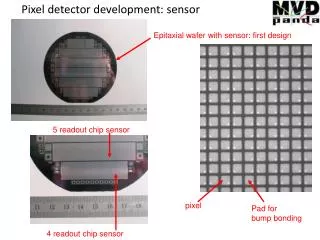
Development of Sensor Board for 802.11 DPAC. BLOCK DIAGRAM. Antenna. RS 232 PC. UCSD Network. Output DPAC WIFI MODULE Input. Humidity Temp Sensor SHT75. GPS Lassen IQ GSP Receiver. CO/NO2 Sensor MiCS-4514. Solar Radiation Sensor Li-200SA. Solar Panel Current Monitor.

E N D
BLOCK DIAGRAM Antenna RS 232 PC • UCSD Network Output DPAC WIFI MODULE Input Humidity Temp Sensor SHT75 GPS Lassen IQ GSP Receiver CO/NO2 Sensor MiCS-4514 Solar Radiation Sensor Li-200SA Solar Panel Current Monitor Battery Voltage Monitor
HARDWARE DESCRIPTION • The sensor board contains the hardware and firmware components required to implement a full Wi-Fi –compatible IEEE 802.11b network interface. • It concludes 4 main sections: * The inputs * DPAC * The Outputs * Power Supply
The Inputs • The inputs are divided into two groups. • The group of the sensors include SHT75, MiCS 4514, GPS, Li200SA. • The group of power monitors include Solar panel current monitor, battery voltage monitor.
The Sensors • These are the weather sensors • The sensor output signals includes two groups: * Analog output (CO/NO2, Solar Radiation Sensor) * Digital output (GPS, Humidity Temp SHT75 sensor) • These sensors connect with the board via the connectors
Lassen iQ GSP receiver Module Mounting: • It uses a single 8-pin (2x4) male header connector (Samtec-ASP 69533-01) for both power and data I/O. • It is mounted on our sensor board by surface-Mount Mating Connector (Samtec- CLP-104-02). • There are four mounting solder tabs on the bottom of the enclosure for securing it on the PCB.
Cont. • RF Connector: - The RF connector mounted on the Lassen iQ GPS receiver is a Hirose Connector( H.FL-R-SMT (10) 50 Ohm). • GPS Antennas: - The antenna receives the GPS satellite signals and passes them to the receiver. The GPS signals are spread spectrum signals in the 1575 MHz range and do not penetrate conductive or opaque surfaces.
Cont: • The Ultra-Compact Embedded GPS Antenna with an HFLconnector, is ideal for portable and mobile applications.
Cont. • Power Requirements: -The Lassen iQ GPS module requires +3.3 VDC ±0.3 VDC at 33 mA, typical excluding the antenna. • Battery Back-up: -The Lassen iQ GPS receiver provides an input for battery back-up (BBU) from 2.5V to 3.6V power to keep the module's RAM memory alive and to power the real-time clock when the receiver's prime power is turned off. - RAM memory is used to store the GPS almanac, ephemeris, and last position.
Cont. • Digital IO/Power Connector Pinout:
Li-Cor #LI-200SA Pyranometer • Measures total solar radiation • Measures direct and reflected solar radiation • mounts to tower with custom NRG side mounting boom and hose clamps • Sensor range from 0 to 3000W/m2
Output signal: - small current signal proportional to total solar radiation (90 μA per 1000 Watts/m2) - range from 0 μA to 270 μA (typical) Measurement: - Converts small current signal output into differential ended voltage output by using Rload =100 Ohm - Uses chip INA 122UA to convert into single ended Voltage to connet to DPAC - With Rf=2.4KOhm, - Chip Gain = 5+200k/2.4K=88.33. - Voutmax= 270*10^-6*100*88.33 = 2.385V SR Power =( Vout*10^6)/(9*88.33)
Solar Panel Current Monitor • Uses monitor current circuit via the voltage across an external sense resistor. • Chooses chip LTC6102 with analog Voltage output to connect with DPAC, V offset= 10MicroV R sense = 0.001Ohm, Rin=3 Ohm, Rout = 2.49 K Ohm • I sense = Vout* Rout / (R sense*Rin)
Battery Voltage Monitor • Max DPAC analog input Voltage is 2.5V • Max Battery Voltage = 12V*1.2=14.4V. • Need to build Voltage divider for this input: R1=18KOhm R2=2KOhm V-Bat V Bat = 10*V in V in GND DPAC
DPAC Airborne Module • Highly integrated 802.11b wireless module with radio, base-band & application processor • Built-in web server enables drop-in LAN and internet connectivity • Configurable serial, digital and analog I/O ports
DPAC Specifications • Technology : . IEEE 802.11b DSSS, Wi-Fi compliant • Frequency: . 2.400 – 2.4835 GHz (US/Can/Japan/Europe) • Modulation: . DBPSK (1 Mbps), DQPSK (2 Mbps), and CCK (5.5 and 11 Mbps) • Clock Frequencies: . 4.8 MHz – CPU reference clock . 32.768 KHz – real-time clock • Channels .USA/Canada: 11 channels (1 – 11) • Data Rate: . 11, 5.5, 2, 1 Mbps (raw wireless rate) • MAC : . CSMA/CA with ACK, RTS, CTS • RF Power: . +15 dBm (typical) Approx.32 mW • Sensitivity: . -82 dBm for 11 Mbps .-86 dBm for 5.5 Mbps .-88 dBm for 2 Mbps .-90 dBm for 1 Mbps
Security WEP standard encryption, 64 or 128 bits • Antenna: . Two U.FL coaxial connectors, 50Ω, supports receive diversity • Supply : 3.3 VDC • Current Consumption: 420 mA – transmit mode (typical) 350 mA – receive mode (typical) 250 mA – doze mode (typical – see Note 1 and Note 5 below) 235 mA – snooze mode (typical – see Note 1 and Note 5 below) 50 mA – sleep mode (typical – see Note 5 below) • Power Up Inrush Current 1900 mA (max) • Operating Temperature Industrial: -40°C − +85°C (see Note 2 below) • Application Processor 16-bit, 120 MIPS @ 120 MHz • Serial Interface • Memory: Flash: 64 Kbytes onboard, 512 Kbytes expansion (see Note 4 below) SRAM: 20 Kbytes onboard, 128 Kbytes expansion • Digital I/O Up to 8 digital I/O ports and status • Analog Inputs Up to 8 channels, 10-bit resolution, single ended, 0 – 2.5 V • Connector 36 pin (pn: HRS DF12-36DS-0.5 V) 4-mm height
The outputs • There are two outputs for this board. • It includes : - External antenna: DPAC Module has two U.Fl style connectors for connection to anntena. These two connectors provide 50 Ohm impedance RF signals at 2.4GHz) - RS 232 Connector: DPAC Module has up to 512 KB Flash memory and 128 KB Static Random Acess Memory to support its function and features.
POWER SUPPLY SP Current Monitor LTC6102 +12V_SP +12V_SP Solar Panel R-Sense Unisolar Us-5 5W 12V Thin film Module +5v DC to DC Switch Converter LM2673S-5.0 +12V ChargeController +5V Discharged Battery +12V_Batt +12V Charged 12V, 5 Ah -Battery +3.3v DC to DC Linear Converter LP3962ES-3.3 Batt Voltage Monitor Voltage Divider +3.3V
Power Sources • The sensor board is powered from the 12V charge controller. • The 12V charge controller can derive power from either Unisolar Us-5 5W, 12V Thin film Module solar panel or 12V, 5 Ah -battery. • The charge controller will protect our batteries from being overcharged by our solar panels and it will block any reverse current as well.
Power Supplies • The sensor board is supplied power from +12V charge controller. • It derives its 5V and 3.3V supplies using onboard regulators • The 5 V power supply is based on an LM2673S-5.0 switching regulator. • The 3.3 V power supply is derived from the 5 V supply using a Series LDO (LP3962ES-3.3) regulator. • These two power supplies are used for DPAC and the sensor power.
Power Schematic • Power Schematic
DPAC SCHEMATIC • DPAC SCHEMATIC
SHT75 SCHEMATIC SHT75 SCHEMATIC
Monitor Schematic • Monitor Schematic
GPS and LI200SA SCHEMATIC • GPS and LI200SA SCHEMATIC
RS232 and CO/NO2 Schematic • RS232 and CO/NO2 Schematic
PCB Layout • PCB Layout
Additional Board • The sensor board will be installed inside the box to protect it from the weather condition. • Outside board is designed and installed outside the box to mount some components that they can not be inside such as CO/NO2 sensor. • It includes MiCS 4514(CO/NO2) sensor, SMA, RS232 connector.
Outside Board Schematic • Outside Board Schematic