Black Pad Defect
Black Pad Defect. Presented By Jodi A. Roepsch. Raytheon NCS TX Engineering McKinney, Texas. Jan 23, 2009. Presentation Outline. Background of Black Pad Defect Failure History of Component Sample Preparation/Experimental Results of Failure Analysis of Failed Component

Black Pad Defect
E N D
Presentation Transcript
Black Pad Defect Presented By Jodi A. Roepsch Raytheon NCS TX Engineering McKinney, Texas Jan 23, 2009
Presentation Outline • Background of Black Pad Defect • Failure History of Component • Sample Preparation/Experimental • Results of Failure Analysis of Failed Component • Exam of Attached Component from Failed PWB • PWB Failures • Factors that Influence the Occurrence of Black Pad Defect • Summary/Conclusion
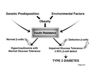
Black Pad Defect can result with Immersion gold/Electroless nickel plating finish. • Hyper-corrosive activity in Immersion gold plating bath. • Results in phosphorus-rich layer. • Term black pad originates from the visual appearance of a surface with the defect. • In the final product, can only be identified destructively. • BGA’s from stock can be examined if gold layer is etched.
Black pad identification: • Mud-cracked appearance. • Abnormally thick phosphorus-rich layer. • Some degree of a phosphorus-rich layer is expected in a normal solder joint. • Corrosion spikes along nickel grains. • Corrosion spikes can act as stress concentration points which can cause cracks in the intermetallics. • Different levels of severity of the defect have been identified ranging from no adverse effect to solder joint reliability to non-wetting of nickel surface and/or premature failure of joint. • Unique to this work is the identification of Cu/Sn IMC formation due to the severity of corrosion spikes penetrating through the Ni/P plating.
Immersion gold plating process • Immersion gold plating process involves galvanic displacement. • Gold ions in solution accept electrons from nickel due to difference in galvanic potential. • Gold is thereby deposited onto surface. • Nickel goes into solution. • Self limiting process by nickel diffusion.
Advantages of ENIG Plating • Ideal for fine pitch features • Flat finish, highly uniform • Ability to survive multiple soldering cycles • Excellent solderability, Pb free compatible • Corrosion resistance • Long shelf life • Diffusion barrier characteristics • Conductivity • Wire bondable surface
Disadvantages of ENIG Plating • Black Pad Defect • Occurrence of defect unpredictable • Difficult to control fabrication process • Latent interfacial fracture failures
Plating stackup on failed BGA’s (Ball Grid Arrays) is electroless nickel-immersion gold. Copper present below the electroless nickel. PWB’s with BGA’s were mechanically stressed. Separation occurred between the solder balls and BGA component pads. Fracture Location BGA Component Solder Balls PWB
Sample Preparation/Experimental • Surface optical exam of failed components. • SEM/EDS analysis of surface. • Microsectioning of failures. • SEM/EDS exam of microsections.
Top of solder balls left on CCA at the time of failure. Fracture surface has a flat appearance.
SE SEM image of interface on solder ball following separation.
BSE SEM image of solder ball surface on PWB after separation. • Cu/Sn intermetallics present.
BGA pad on component has a mud-cracked appearance indicative of black pad defect.
Low magnification image of pad with defect. The surface contains areas of solder, Cu/Sn intermetallics, and non-wetted mud-cracked Ni surface.
Mud-cracked surface where solder did not wet Cu/Sn IMC’s Ni/P surface, solder did not wet in this area
Elemental map of area seen in SEM image in the upper left corner. Cu/Sn intermetallics and non-wetted surface present.
Non-wet surface with some corrosion spikes along the nickel grains.
Solder has a dimpled appearance. Sn alloying with the Cu from the pad below the Ni/P plating.
Dimpled area of solder when viewed from surface. Several locations have the defect.
Severe black pad defect present. Copper/Tin intermetallics present above nickel layer. Path present between solder and copper pad via corrosion spikes.
EDS elemental map of defect area. Cu/Sn intermetallics present above nickel plating.
Gold removed from BGA from stock from different supplier. The dark region surrounding mud-cracks indicate high phosphorus areas.
Cross-sectional view of failed pad. Corrosion spikes extend into nickel below phosphorus-rich layer.
Phosphorus weight percent in black pad region. Phosphorus weight percent in good area of nickel.
Summary of Failed Component • Failed surfaces have a flat appearance. Evidence of a brittle fracture as well as non-wetting of the solder. • Immersion gold/Electroless nickel plating finish. • Severe black pad detected on failed components. • Mud-cracked appearance from surface. • Phosphorus-rich layers. • Corrosion spikes extending through Ni layer to underlying Cu. • Cu/Sn intermetallics detected above Ni layer. • Many BGA pad surfaces show non-wetting to Ni/P. Majority of attachment is by Cu/Sn IMC formation through corrosion spikes. • Intermetallics are brittle and therefore less likely to withstand mechanical shock. • Corrosion cracks in nickel layer below Ni/Sn intermetallics known to act as stress risers increasing likelihood of cracks/fracture in intermetallics.
Image of pad to ball interface on component side. Severe crack present at solder to phosphorus-rich black pad interface. Little to no Ni/Sn intermetallics formed.
Elemental map of crack between the Cu/Sn intermetallics and Nickel plating interface.
Cu/Sn intermetallics formed on surface of Ni plating. Micro-cracks initiating at intermetallics. Little to no Ni/Sn intermetallics present. Cu/Sn intermetallics formed primary bond to pad anchoring the solder ball.
Cu/Sn intermetallics present. • Cu/Sn forms primary bond between solder ball and pad. • Little to no Ni/Sn intermetallics formed.
Summary of Attached Component • Black pad defect present. • Cu/Sn intermetallics present similar to failed component. • Severe cracking present between nickel plating and Cu/Sn intermetallics at interface. • Cu/Sn intermetallics anchoring solder ball to component pad. • Micro-cracks present initiating at Cu/Sn intermetallics where solder ball attached to pad.
PWB Failure History • Populated board submitted to FAL due to dewetting of the solder at the plated through holes (PTH). • After several reworks, solder still did not wet. • Optical exam of the PTH indicated a black surface present. • SEM exam showed a mud-cracked surface. • EDS analysis indicated a high phosphorus content in the dark regions.
Solder has dewetted in the dark regions. • Corrosion spikes present along the nickel grains.
Quant Data from PTHs Image 1 Image 2 Image 3 Image / Spectrum P wt% Image 1 Spectrum 1 15.1 Image 2 Spectrum 1 13.9 Spectrum 2 13.0 Image 3 Spectrum 1 18.5 Spectrum 2 17.7 Spectrum 3 14.8
Conditioned versus Unconditioned Coupons • Coupons compared to determine effect of processing on the black pad defect. • Conditioning process • Wash • Baked 72 hours @ 105C, normally done for 8 hours • Reflow oven (1 cycle) • Wash • No significant differences observed between conditioned and unconditioned coupons.
Condition Coupon Etch Run
Conditioned Coupon Etch Run Filled Via
Reliability Concerns • Black pad defect in most cases can only be detected with destructive analyses. • May cause latent failures. • Corrosion spikes can concentrate stress to the brittle intermetallics causing a premature failure. • In severe cases, possible to form Cu/Sn intermetallics which can anchor a component to a PWB. A weak or marginal joint may go unnoticed until time of latent failure. • No screening tests available for the black pad defect. • Occurrence of the defect is random and unpredictable. It is not lot specific.