Technology Overview
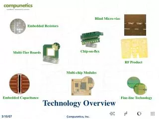
Multi-chip Modules. Fine-line Technology. Blind Micro-vias. Embedded Resistors. Chip-on-flex. Multi-Tier Boards. RF Product. Embedded Capacitance. Technology Overview. Agenda. Corporate Overview Compunetics, Inc. Company Profile Standard Technologies Challenging Technologies

Technology Overview
E N D
Presentation Transcript
Multi-chip Modules Fine-line Technology Blind Micro-vias Embedded Resistors Chip-on-flex Multi-Tier Boards RF Product Embedded Capacitance Technology Overview
Agenda Corporate Overview Compunetics, Inc. Company Profile Standard Technologies Challenging Technologies Extreme Technologies Samples Questions
Corporate Overview • 30+ Years Experience in Design, Development and Manufacture of Highly-sophisticated Electronic Systems • Telecommunications, Medical, Industrial, Transportation and Government Markets • Internal Control over Manufacturing • 330+ Employees
Corporate Overview Compunetix, Inc. Compunetics, Inc. Chorus Call, Inc. Instrumentation Systems Division Chorus Call, Inc. USA Communication Systems Division Printed Circuit Board Group Chorus Call International Switzerland Germany Italy India South Africa Greece Brazil Canada Australia Video Systems Division Federal Systems Division
PCB Layout & Design To Handle Customer Design Overflow And To Give Support To Customer’s Design Group Engineering Group Consisting Of 8 Engineers Dedicated To Managing / Fabricating Critical Or Technologically Challenging Projects Company Profile Compunetics, Inc. Manufacturing Sales / Marketing Quality Services Engineering Services Engineering Production Global Products Company Differentiators
Company Profile • SBA/FAR 19 Small Business • 38 Years Experience Producing Complex Interconnect Systems • Customers in Commercial, Education, Telecommunication, and Government Markets • Independent Internal R&D • 2006 Revenues: $11.0 Million • 80+ Employees • 25+ Engineers and Professionals • ISO9001:2000 Registered and MIL Spec Certified
Company Profile Quality Certifications ISO 9001:2000 Registered UL Certified for Single / Double Sided and Multilayer Boards MIL-P-55110 Certified for FR4, Polyimide General Dynamics Land Systems Certified for Prototypes and Production Hamilton Sundstrand Space Certification JPL / NASA Flight Certified General Dynamics UK Award For “Best Overall Business Performance 2004 / 2005”
Company Profile Types of Business Prototypes, Quick Turn & Small To Medium Production Military Spec PCBs Rigid, Flex & Rigid/Flex (Class 2, 3 & Mil Spec) High Layer Count – Up to 30 Layers, High Density PCBs Independent Design/Drafting Group Buried Passives High Density Interconnects Multi Chip Modules, Chip-On-Board Engineering / Design Assistance
Company Profile Customer Base Orbital DRS Northrop Grumman Terumo Raytheon L3 Communications Philips Medical Maxtek David Sarnoff Bombardier Teledyne General Dynamics Lockheed Martin DoD / DoE IBM Harris Intel Tektronix • Land Systems • United Kingdom • AIS • ATP
Standard Technologies Technology Can Be Purchased In Volumes Overseas Most US Board Shops Can Produce
Standard Technologies Board Material: High Tg FR4 Layer Counts 2 to 12 Layers Trace / Space - .005 / .005 on 1 oz. Copper Trace / Space - .004 / .004 on 1/2 oz. Copper (inner) BGA’s 1.0 mm IPC Class 2 Build Specification Aspect Ratios of < 6:1
Challenging Technologies Technology Can Be Purchased In Volumes Overseas From Select Few Sources Few High End US Board Shops Can Produce
Challenging Technologies Board Material: Polyimide, Flex, High Speed FR4, Ceramic Filled Materials, Teflon Layer Counts Up To 26 Layers Trace / Space - .004 / .004 on 1 oz. Copper Trace / Space - .003 / .003 on 1/2 oz. Copper (inner) Trace / Space - .004 / .004 on 1/2 oz. Copper (outer) BGA’s 0.8 mm IPC Class 3 Build Specification or Mil-Spec Aspect Ratios of < 10:1
Challenging Technologies Embedded Passives (Resistors) • A True Thin-Film, Nickel-Phosphorous (NiP) Alloy. • About 0.1 To 0.4 Microns Of The Alloy Is Electro-Deposited On To The Rough, Or Tooth Side Of Copper Foil During Manufacturing • Typical Tolerance Of 10 – 20% • Resistors Tested At Final Test And During Inner Layer OHMEGA-PLY LAMINATE copper resistive material (0.1-0.4 micron thick) dielectric substrate copper (EXAMPLE OF AVAILABLE CORE)
CURRENT OUT CURRENT IN COPPER COPPER NICKEL RESISTOR NICKEL RESISTOR NICKEL RESISTOR DIELECTRIC SUBSTRATE DIELECTRIC SUBSTRATE DIELECTRIC SUBSTRATE Challenging Technologies Embedded Passives (Resistors) • ELECTRIC CURRENT FLOWS THROUGH THE LEAST RESISTIVE MATERIAL • COPPER NICKEL COPPER
Challenging Technologies Embedded Passives (Resistors) • Increased Active Circuit Density • Replaces Discrete Resistors • Incorporated Within The Board • Can Be Placed Under Components • Ability To Reduce Board Size • Weight Savings • Double Sided SMT May Be Converted To Single Sided SMT • Improved Electrical Performance • Significantly Reduced Signal Path To Resistors • Termination Of All Signals Become Possible • Low Inductance (Less Than 0.7 nH TYPICAL) • Reduced Surface EMI
Challenging Technologies Embedded Passives (Resistors) • Improved Reliability • Elimination Of Solder Joints • Excellent Long Term (Trillions Of Component Hours Of Operation) Reliability In Millions Of Circuit Boards In Computer, Consumer, Military And Telecommunications Applications • Cost Savings • Elimination Of Discrete Resistors • Rework Reduction • Board Density and/or Size Reduction
Challenging Technologies Embedded Passives (Resistors) Applications Series Termination
Challenging Technologies Embedded Passives (Resistors) Applications Parallel Termination
Cu Film Core Cu Copper clad laminate Double sided (power and ground) Dielectric is a Polyimide and BaTiO composite. Thickness of dielectric is key…thinner is better Challenging Technologies Embedded Passives (Capacitors) • Bulk Capacitance Formed By Placing Power And Ground Layers Close Together • Thin Dielectrics Separate Power And Ground To Create Parallel Plate Capacitor C = keA/t Where: C = Capacitance e = Dielectric Constant of Material A = Board Area in Square Inches k = Permittivity of Free Space – Constant of 225 t = Dielectric Thickness in inches
Challenging Technologies Embedded Passives (Capacitors) • Reduction In SMT Caps Needed On PCB • Closely Spaced Planes Have Lower Inherent Inductance Therefore Supply Current On A Very Short Time Scale Thus Damping Fluctuations Of Voltage At Device Input • Low Inductance Planes Reduces EMI • Initial Data Indicates That Surface Mounted Capacitance Can Be Effectively Replaced By Embedded Capacitance With Only A Small Fraction Of The Total Discrete Capacitance
Challenging Technologies Embedded Passives (Capacitors) Products
Challenging Technologies Embedded Passives (Capacitors) Application • Before Embedded Capacitance • 18 Layers • Blind vias: 1-2, 18-17 • Buried vias 2-17 • Over 2000 Caps • After Embedded Capacitance • 18 Layers • No Blind Vias • Buried vias 2-17 • Removed 800+ Caps
Challenging Technologies Controlled Impedance Flex • Faster Signals with Faster Rise/Fall Times Require Controlled Impedance Flex Cables • In Order To Have Cable Flexible, Need To Etch Traces Near 3 mils (Larger Traces Require Thicker Dielectrics For Same Impedance, Making Board Less Flexible) • Controlled Impedance Flex • 8 Layers • Trace / Space – 3.5 / 3.5 • DuPont AP & LF Flex Material • Differential Controlled Impedance
Challenging Technologies Rigid-Flex • Common Application To Add Reliability And/Or To Reduce Assembly Costs Through Removal Of Connectors And Cabling • More Common Due To Tight Spaces And Need For Increased Reliability In Products, Especially In Military • Military Avionics Rigid Flex • 8 Layers • 2 oz. Copper • Loose-leaf Design for Increase Flexibility • 3 Double Sided Flex Cores w/Coverlay • Military Specification
Challenging Technologies Rigid-Flex • Satellite Systems • 12 Layers • Flight Certified Product • Polyimide / DuPont AP Flex • Immersion Gold • Military • 22 Layers • 6 Layer Loose-leaf Flex • Polyimide / DuPont AP Flex • HAL Finish
Challenging Technologies High Speed – Mixed Material Boards • Need For Low Df/Dk Materials for Today’s Technology • Mix Low Df/Dk, High Cost Material with Higher Df/Dk Low Cost Material • Keep Critical Signals on/with Low Df/Dk Material • Some Materials can not be Mixed with Certain Other Materials • Mixed Material 10Gb Ethernet • 8 Layers • Blind Vias – 1-4 For Stub Control • Conductive Epoxy Filled Vias • Rogers 4003 / FR4 Material • Cavity Construction at Gold Fingers
FR4 Material (Glass Bundles) • Rogers 4000 (Ceramic Filled) Challenging Technologies High Speed – Mixed Material Boards
Challenging Technologies Heat Dissipation Boards • Smaller Spaces and Hotter Running Parts Require Design Consideration for Heat Dissipation • Need To Provide Thermal Path Away From Components • Several Design Changes Can be Made To Minimize Thermal Impact to Components • Place Heat Generating Part Near Heat Sink or Board Edge • Provide Thermal Path In Copper Including Using Edge Plating • Use Thermal Vias to Connect to Internal Planes or Heat Sink • Use of CB100 for Thermal Vias • Heat Sinks • Thinner Board Materials Place Component Closer To Heat Sink
Challenging Technologies Heat Dissipation Boards • Heat Dissipation Board • 4 Layers • Thin Core FR4 • Conductive Epoxy • Heat Spreader Attached w/ Thermagon • HASL Finish
Challenging Technologies RF Boards • Boards Typically Made on Teflon or Teflon Blend Products • Etching Tolerance of +/- .0005” • Several Areas of Tight Tolerance Routing +/- .002 (Requires Laser Routing w/Vision System • Some Designs Require Metal Backing • Most Require Wirebondable Gold
Challenging Technologies RF Boards • Commercial RF • 2 Layers • Rogers 3003 • Laser Routed Slots • Trace Tolerance +/- .0003” • Wirebondable Gold • Military RF • 4 Layers • Rogers 6002, 4350, 4403 • Blind 1-2, 4-3; Buried 2-3 • Cavity 4 to 3 • Trace Tolerance +/- .0003” • Wirebondable Gold
Challenging Technologies Laser Drilled Blind Micro-vias • Typically .004” to .006” Laser Drilled Hole From Layers 1 to 2 and/or From N to (N-1) • Dielectric Distance .003” to .004” • Aspect Ratios less than .50:1 • Material Typically RCC (Resin Coated Copper) or Flat Glass FR4 • Enables Pin Escaping Small Pitch BGAs or BGAs on Thick PCBs • Used to Conserve Routing Channels on Inner Layers • Enables Double Sided Assembly in Some Cases
Challenging Technologies Laser Drilled Blind Micro-vias
Extreme Technologies Overseas Supply Limited to Japan Very Few US Board Shops Can Produce Some Technology Still Under Development
Extreme Technologies Chip On Flex (Direct Die Attach) • Chip On Flex • 2 Layers • Trace / Space – 2 / 2 • 2 mil Laser Drilled Vias • Wirebondable Gold • 2 mil Adhesiveless Pyralux
Extreme Technologies Buried Resistors on Flex • Buried Resistor on Flex • 2 Layers • Ohmega Ply Resistor • Resistor Covered By Kapton • Immersion Silver Finish • 2 mil Adhesiveless Pyralux
Extreme Technologies Laser Trimmed Embedded Resistors • Laser Trimmed Resistors • Resistor Laser Trimmed Under Measurement • Resistor Trimmed to +/- 1% • Final Resistor Tolerance +/- 3% • Application: High Speed Testing
Extreme Technologies Copper Filled Micro-vias • Via-in-pad Provides Flat Pad Surface for BGA Attach • Flat Surface Optimal For Stacked Micro-vias • Need For Special Plating Chemistry • Need For Special Plating Equipment • Enables Pin Escaping High Pin Count .5 mm Pitch BGAs • Technology Under Development at Several US Shops
Extreme Technologies Copper Filled Micro-vias Current Plating Technology
Extreme Technologies Copper Filled Micro-vias Compunetics Test Results • Test Boards Have Been Received From (2) Chemistry Manufacturers • The Smaller The Hole, The More Flat the Plating • Plating of Close to 1:1 on Blind Microvias • Both Manufacturers to Receive Stacked Microvia Tests • Stress Testing In Progress
Extreme Technologies Copper Filled Micro-vias Stacked Micro-vias
Extreme Technologies Copper Filled Micro-vias Stepped Micro-vias
Extreme Technologies High Aspect Ratio Blind Micro-via Plating • Some Designs Require More Dielectric Between Layers 1-2 and Still Require Blind Micro-vias • Current Technology at approx. 0.7:1 Aspect Ratio • Industry Looking for Aspect Ratios of Greater Than 1.25:1 • Copper Filled Micro-via Chemistry and Equipment May Help Increase Achievable Aspect Ratios
Extreme Technologies DuPont PF Material • All Polyimide Adhesive • Flex “prepreg” Without Acrylic • Lower Z-axis Expansion Without Acrylic • Increase Reliability • Much Lower Df (.02 vs. .004) • Product Withstands MIL-Spec Thermal Shock Testing • Product Still In Beta-Test at Several Shops Including Compunetics, Inc. • Evaluations On-going at Several Large OEMs
Extreme Technologies DuPont PF Material Multi-Layer Flex w/ PF Material Multi-Layer Flex w/ LF Bondply
Extreme Technologies Fine Line Technology (2 mil Trace/Space & Down) • Required for High Pin Count Fine Pitch BGA Routing (<= 0.5 mm Pitch) • Chip On Board / Chip On Flex • Used To Reduce Layer Count – More Tracks per Channel • Seen with Laser Drilled Micro-vias • Typically on Boards with Small Annular Rings • Can be Combined with Embedded Passives
Extreme Technologies Laser Ablation Of Soldermask Problem • Tighter Pitch Parts Require Better Soldermask Registration • Conventional Mask Annular Rings Leave Insufficient Mask Dams • BGA Area Covered With Soldermask • YAG Laser Used To Remove Mask From BGA Pads • Mask Annular Ring Less Than 1 mil • Mask Dams Remain Aiding Assembly Solution
Extreme Technologies Fine Line Technology (2 mil Trace/Space & Down) • Multi-Level Chip Package • 6 Layer FR4 • 2 / 2 Trace / Space • Embedded Resistors for Termination • Multi-Level Cavity Construction • Wirebondable Gold • Fine Line Package • 1.5 / 1.5 (35 / 35 um) Trace / Space • Wirebondable Gold • 4 Layers FR4 • 31 mil Thick +/- 1 mil
Extreme Technologies Ink Jet Printing • Technology Under Development • Printing of: Legend and Soldermask (Near Production) • Printing of: Conductors, Resistors, Inductors, etc. (In Development) • Advantage: Finer Placement of Material Yields Tighter Tolerance and Finer Features • Several Board Shops Helping Industry Develop Technology • Inkjet Technology Also Under Development at Several Universities • RFID Technology – Blind Via Fill