CMOS Inverter: Dynamic
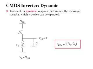
CMOS Inverter: Dynamic. Transient, or dynamic , response determines the maximum speed at which a device can be operated. V DD. V out = 0. C L. t pHL = f(R n , C L ). R n. V in = V DD. Sources of Resistance. MOS structure resistance - R on Source and drain resistance

CMOS Inverter: Dynamic
E N D
Presentation Transcript
CMOS Inverter: Dynamic • Transient, or dynamic, response determines the maximum speed at which a device can be operated. VDD Vout = 0 CL tpHL = f(Rn, CL) Rn Vin = V DD
Sources of Resistance • MOS structure resistance - Ron • Source and drain resistance • Contact (via) resistance • Wiring resistance Top view Poly Gate Drain n+ Source n+ W L
VGS VT Ron D S MOS Structure Resistance • The simplest model assumes the transistor is a switch with an infinite “off” resistance and a finite “on” resistance Ron • However Ron is nonlinear, so use instead the average value of the resistances, Req, at the end-points of the transition (VDD and VDD/2) Req = ½ (Ron(t1) + Ron(t2)) Req = ¾ VDD/IDSAT (1 – 5/6 VDD)
x105 (for VGS = VDD, VDS = VDDVDD/2) Req (Ohm) VDD (V) Equivalent MOS Structure Resistance • The on resistance is inversely proportional to W/L. Doubling W halves Req • For VDD>>VT+VDSAT/2, Req is independent of VDD (see plot). Only a minor improvement in Req occurs when VDD is increased (due to channel length modulation) • Once the supply voltage approaches VT, Req increases dramatically Req (for W/L = 1), for larger devices divide Req by W/L
Source and Drain Resistance G • More pronounced with scaling since junctions are shallower • With silicidation Ris reduced to the range 1 to 4 / D S RS RD RS,D = (LS,D/W)R where LS,D is the length of the source or drain diffusion R is the sheet resistance of the source or drain diffusion (20 to 100 /)
Contact Resistance • Transitions between routing layers (contacts through via’s) add extra resistance to a wire • keep signals wires on a single layer whenever possible • avoid excess contacts • reduce contact resistance by making vias larger (beware of current crowding that puts a practical limit on the size of vias) or by using multiple minimum-size vias to make the contact • Typical contact resistances, RC, (minimum-size) • 5 to 20 for metal or poly to n+, p+ diffusion and metal to poly • 1 to 5 for metal to metal contacts • More pronounced with scaling since contact openings are smaller
Wire Resistance L L R = = A H W Sheet Resistance R L R1 = R2 H = W
Skin Effect • At high frequency, currents tend to flow primarily on the surface of a conductor with the current density falling off exponentially with depth into the wire W • = (/(f)) where f is frequency = 4 x 10⁻⁷ H/m so the overall cross section is ~ 2(W+H) • = 2.6 m for Al at 1 GHz H • The onset of skin effect is at fs - where the skin depth is equal to half the largest dimension of the wire. fs = 4 / ( (max(W,H))2) • An issue for high frequency, wide (tall) wires (i.e., clocks!)
Skin Effect for Different W’s for H = .70 um 1E8 1E9 1E10 • A 30% increase in resistance is observed for 20 m Al wires at 1 GHz (versus only a 1% increase for 1 m wires)
The Wire transmitters receivers schematic physical
Wire Models • Interconnect parasitics (capacitance, resistance, and inductance) • reduce reliability • affect performance and power consumption All-inclusive (C,R,l) model Capacitance-only
Parasitic Simplifications • Inductive effects can be ignored • if the resistance of the wire is substantial enough (as is the case for long Al wires with small cross section) • if the rise and fall times of the applied signals are slow enough • When the wire is short, or the cross-section is large, or the interconnect material has low resistivity, a capacitance only model can be used • When the separation between neighboring wires is large, or when the wires run together for only a short distance, interwire capacitance can be ignored and all the parasitic capacitance can be modeled as capacitance to ground
Simulated Wire Delays L Vin Vout L/10 L/4 L/2 L voltage (V) time (nsec)
RDriver Vout Clumped Driver Vout cwire capacitance per unit length Wire Delay Models • Ideal wire • same voltage is present at every segment of the wire at every point in time - at equi-potential • only holds for very short wires, i.e., interconnects between very nearest neighbor gates • Lumped C model • when only a single parasitic component (C, R, or L) is dominant the different fractions are lumped into a single circuit element • When the resistive component is small and the switching frequency is low to medium, can consider only C; the wire itself does not introduce any delay; the only impact on performance comes from wire capacitance • good for short wires; pessimistic and inaccurate for long wires
(r,c,L) Vin VN rL rL rL rL rL Vin VN cL cL cL cL cL • Delay is determined using the Elmore delay equation Di = ckrik N k=1 Wire Delay Models, con’t • Lumped RC model • total wire resistance is lumped into a single R and total capacitance into a single C • good for short wires; pessimistic and inaccurate for long wires • Distributed RC model • circuit parasitics are distributed along the length, L, of the wire • c and r are the capacitance and resistance per unit length
2 r2 c2 r1 s 1 r3 4 r4 c4 c1 3 ri c3 i ci • Path resistance (sum of the resistances on the path from the input node to node i) rii = rj (rj [path(s i)] i j=1 • Shared path resistance (resistance shared along the paths from the input node to nodes i and k) rik = rj (rj [path(s i) path(s k)]) N j=1 • A typical wire is a chain network with (simplified) Elmore delay of DN = cirii N i=1 RC Tree Definitions • RC tree characteristics • A unique resistive path exists between the source node and any node of the network • Single input (source) node, s • All capacitors are between a node and GND • No resistive loops
N i Elmore delay equation DN = cirii = ci rj Chain Network Elmore Delay D1=c1r1 D2=c1r1 +c2(r1+r2) r1 r2 ri-1 ri rN 1 2 i-1 i N VN Vin c1 c2 ci-1 ci cN Di=c1r1+c2(r1+r2)+…+ci(r1+r2+…+ri) Di=c1req+2c2req+3c3req+…+icireq
Elmore Delay Models Uses • Modeling the delay of a wire • Modeling the delay of a series of pass transistors • Modeling the delay of a pull-up and pull-down networks
Distributed RC Model for Simple Wires • A length L RC wire can be modeled by N segments of length L/N • The resistance and capacitance of each segment are given by r L/N and c L/N DN = (L/N)2(cr+2cr+…+Ncr) = (crL2) (N(N+1))/(2N2) = CR((N+1)/(2N)) where R (= rL) and C (= cL) are the total lumped resistance and capacitance of the wire • For large N DN = RC/2 = rcL2/2 • Delay of a wire is a quadratic function of its length, L • The delay is 1/2 of that predicted (by the lumped model)
Step Response Points • Example: Consider a Al1 wire 10 cm long and 1 m wide • Using a lumped C only model with a source resistance (RDriver) of 10 k and a total lumped capacitance (Clumped) of 11 pF t50% = 0.69 x 10 k x 11pF = 76 ns t90% = 2.2 x 10 k x 11pF = 242 ns • Using a distributed RC model with c = 110 aF/m and r = 0.075 /m t50% = 0.38 x (0.075 /m) x (110 aF/m) x (105 m)2 = 31.4 ns t90% = 0.9 x (0.075 /m) x (110 aF/m) x (105 m)2 = 74.25 ns Poly: t50% = 0.38 x (150 /m) x (88+254 aF/m) x (105 m)2 = 112 s Al5: t50% = 0.38 x (0.0375 /m) x (5.2+212 aF/m) x (105 m)2 = 4.2 ns Time to reach the 50% point is t = ln(2) = 0.69 Time to reach the 90% point is t = ln(9) = 2.2
RDriver rw,cw,L Vout Vin Putting It All Together • Total propagation delay consider driver and wire D = RDriverCw + (RwCw)/2 = RDriverCw + 0.5rwcwL2 and tp = 0.69 RDriverCw + 0.38 RwCw where Rw = rwL and Cw = cwL • The delay introduced by wire resistance becomes dominant when (RwCw)/2 RDriver CW (when L 2RDriver/Rw) • For an RDriver = 1 k driving an 1 m wide Al1 wire, Lcrit is 2.67 cm
Design Rules of Thumb • rc delays should be considered when tpRC > tpgate of the driving gate Lcrit > (tpgate/0.38rc) • actual Lcrit depends upon the size of the driving gate and the interconnect material • rc delays should be considered when the rise (fall) time at the line input is smaller than RC, the rise (fall) time of the line trise < RC • when not met, the change in the signal is slower than the propagation delay of the wire so a lumped C model suffices
Nature of Interconnect Global Interconnect Source: Intel
silicide polysilicon SiO2 + + n n p Overcoming Interconnect Resistance • Selective technology scaling • scale W while holding H constant • Use better interconnect materials • lower resistivity materials like copper • As processes shrink, wires get shorter (reducing C) but they get closer together (increasing C) and narrower (increasing R). So RC wire delay increases and capacitive coupling gets worse. • Copper has about 40% lower resistivity than aluminum, so copper wires can be thinner (reducing C) without increasing R • use silicides (WSi2, TiSi2, PtSi2 and TaSi) • Conductivity is 8-10 times better than poly alone • Use more interconnect layers • reduces the average wire length L (but beware of extra contacts)
IBM CMOS-8S CU, 0.18m - 0.10 M7 - 0.10 M6 - 0.50 M5 - 0.50 M4 - 0.50 M3 - 0.70 M2 - 0.97 M1 Wire Spacing Comparisons Intel P858 Al, 0.18m Intel P856.5 Al, 0.25m - 0.07 M6 - 0.05 M5 - 0.08 M5 - 0.12 M4 - 0.17 M4 - 0.33 M3 - 0.49 M3 - 0.33 M2 - 0.49 M2 - 1.11 M1 - 1.00 M1 Scale: 2,160 nm From MPR, 2000
Comparison of Wire Delays From MPR, 2000
Inductance • When the rise and fall times of the signal become comparable to the time of flight of the signal waveform across the line, then the inductance of the wire starts to dominate the delay behavior • Must consider wire transmission line effects • Signal propagates over the wire as a wave (rather than diffusing as in rc only models) • Signal propagates by alternately transferring energy from capacitive to inductive modes l l l l r r r r Vin Vout c c c c g g g g
More Design Rules of Thumb • Transmission line effects should be considered when the rise or fall time of the input signal (tr, tf) is smaller than the time-of-flight of the transmission line (tflight) tr (tf) < 2.5 tflight = 2.5 L/v • For on-chip wires with a maximum length of 1 cm, we only worry about transmission line effects when tr < 150 ps • Transmission line effects should only be considered when the total resistance of the wire is limited R < 5 Z0 = 5 (V/I)