CMOS Process Integration
CMOS Process Integration. ECE/ChE 4752: Microelectronics Processing Laboratory. Gary S. May March 25, 2004. Outline. Introduction MOSFET Fabrication CMOS Technology Well Formation Advanced Isolation. MOSFET. MOSFET = “Metal-Oxide-Semiconductor Field-Effect Transistor”

CMOS Process Integration
E N D
Presentation Transcript
CMOS Process Integration ECE/ChE 4752: Microelectronics Processing Laboratory Gary S. May March 25, 2004
Outline • Introduction • MOSFET Fabrication • CMOS Technology • Well Formation • Advanced Isolation
MOSFET • MOSFET = “Metal-Oxide-Semiconductor Field-Effect Transistor” • At present, the MOSFET is the dominant device in GSI circuits because it can be scaled to smaller dimensions than other types of devices. • The dominant technology for MOSFET is CMOS (complementary MOSFET), in which both n-channel and p-channel devices are provided on the same chip. • CMOS technology has the lowest power consumption of all IC technology.
MOSFET Scaling • In 1970s, gate length was 7.5 mm and device area was ~ 6000 mm2. • For present-day MOSFETs, the gate length is < 0.10 mm.
Outline • Introduction • MOSFET Fabrication • CMOS Technology • Well Formation • Advanced Isolation
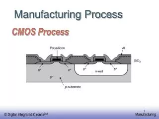
Process Sequence • Start w/ p-type, lightly doped (~1015 cm–3), <100>-oriented Si. • Form oxide isolation region (a). • Define active area with photoresist mask and boron chanstop layer implanted through nitride-oxide layer (b). • Grow gate oxide (< 10 nm) and adjust threshold voltage by implanting B ions (enhancement-mode device) (c). • Form gate by depositing doped polysilicon. Pattern gate in source and drain regions (d).
Process Sequence (cont.) • Implant arsenic (~30 keV, ~5 × 1015 cm–2) to form source and drain (a). • P-glass is deposited and flowed (b). • Contact windows defined and etched in P-glass. Al is deposited and patterned (c). • Top view of completed MOSFET (d).
Outline • Introduction • MOSFET Fabrication • CMOS Technology • Well Formation • Advanced Isolation
CMOS Inverter Schematic • Gate of upper PMOS device connected to the gate of lower NMOS device. • Functions as a digital switch • Low power consumption (~ nW) is most attractive feature
CMOS Processing • p-well is implanted and driven into n-substrate (p-type dopant concentration must be high enough to overcompensate the n-substrate background doping). • Subsequent processes for n-channel MOSFET in p-well are identical to nMOSFET. • For p-channel MOSFET, B ions are implanted into n-substrate to form source and drain • Because of p-well and steps needed for p-FET, the number of steps in CMOS fabrication is double that to make NMOS.
Outline • Introduction • MOSFET Fabrication • CMOS Technology • Well Formation • Advanced Isolation
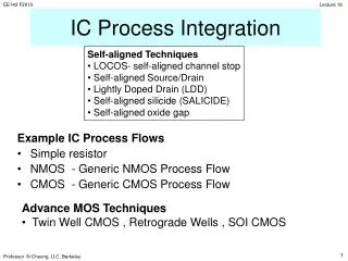
Well Types • Single well – discussed previously • Twin well • p-well and n-well side-by-side on lightly doped substrate • Disadvantage: needs high temperature processing (above 1050 oC) and a long diffusion time (>8 hours) to achieve the required well depth of 2 – 3 mm • Retrograde • To reduce process temperature and time, high-energy implantation is used • The profile of the well in this case can have a peak at a certain depth in the silicon substrate.
Retrograde Wells • Advantages: • Reduced lateral diffusion and increase the device density. • Lower well resistivity • Chanstop can be formed at the same time as well implantation
Outline • Introduction • MOSFET Fabrication • CMOS Technology • Well Formation • Advanced Isolation
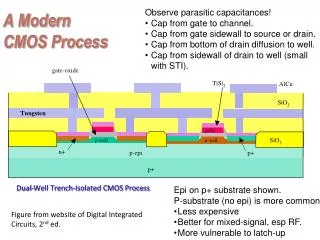
Conventional Isolation • Conventional MOS isolation process has disadvantages for deep-submicron (< 0.25 mm) fabrication: • High-temperature and long oxidation time result in encroachment of chanstop implantation to the active region, causing a threshold voltage shift. • Area of the active region is reduced because of lateral oxidation • Field oxide thickness is significantly less than that grown in wider spacings • Trench isolation technology can avoid these problems.
Shallow Trench Isolation (a) Patterning (b) Trench area etched (c) Trench re-filled with oxide (d) Chemical-mechanical polishing removes the oxide on the nitride to get a flat surface