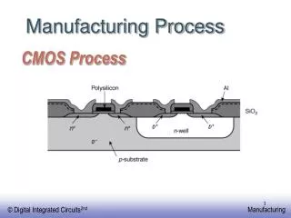
CMOS Manufacturing Process
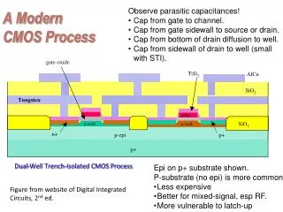
This presentation explores the modern CMOS manufacturing process using a dual-well, trench-isolated approach for a two-inverter circuit. It highlights key manufacturing steps such as photo-lithography, etching, deposition, and implantation. Important cross-sectional constructions like N-well and P-well with details on oxide growth and doping are shown. The slides serve as a snapshot of manufacturing processes in semiconductor design, with references for comprehensive learning available on Fullman's semiconductor site.

CMOS Manufacturing Process
E N D
Presentation Transcript
DD M 2 V in M 1 CMOS Process
A Modern CMOS Process Dual-Well Trench-Isolated CMOS Process
Circuit Under Design This two-inverter circuit will be manufactured in a twin-well process.
The Manufacturing Process These slides only present only a couple of snapshots of the manufacturing process for the circuits presented in the textbook. For a complete overview of all steps, please refer to: http://www.fullman.com/semiconductors/semiconductors.html
Photo-Lithographic Process optical mask oxidation photoresist photoresist coating removal (ashing) stepper exposure Typical operations in a single photolithographic cycle (from [Fullman]). photoresist development acid etch process spin, rinse, dry step
Define active areas Etch and fill trenches Implant well regions Deposit and pattern polysilicon layer Implant source and drain regions and substrate contacts Create contact and via windows Deposit and pattern metal layers CMOS Process at a Glance
Starting wafer: n-type with doping level = 10 13 3 /cm Start Material A A’ * Cross-sections will be shown along vertical line A-A’
N-well Construction (1) Oxidize wafer (2) Deposit silicon nitride (3) Deposit photoresist
N-well Construction (4) Expose resist using n-well mask
N-well Construction (5) Develop resist (6) Etch nitride and (7) Grow thick oxide
N-well Construction (8) Implant n-dopants (phosphorus) m (up to 1.5 m deep)
P-well Construction Repeat previous steps
Grow Gate Oxide 0.055 mm thin
Grow Thick Field Oxide 0.9 mm thick Uses Active Area mask Is followed by threshold-adjusting implants
Contact-Hole Definition (1) Deposit inter-level dielectric (SiO2) — 0.75 mm (2) Define contact opening using contact mask
Aluminum-1 Layer Aluminum evaporated (0.8 mm thick) followed by other metal layers and glass
Define active areas Etch and fill trenches Implant well regions Deposit and pattern polysilicon layer Implant source and drain regions and substrate contacts Create contact and via windows Deposit and pattern metal layers CMOS Process at a Glance
Design Rules • Interface between designer and process engineer • Guidelines for constructing process masks • Unit dimension: Minimum line width • scalable design rules: lambda parameter • absolute dimensions (micron rules)
Layer Color Representation Well (p,n) Yellow Active Area (n+,p+) Green Select (p+,n+) Green Polysilicon Red Metal1 Blue Metal2 Magenta Contact To Poly Black Contact To Diffusion Black Via Black CMOS Process Layers
Intra-Layer Design Rules 4 Metal2 3
Design Rule Checker poly_not_fet to all_diff minimum spacing = 0.14 um.
V DD 3 Out In 1 GND Stick diagram of inverter Sticks Diagram • Dimensionless layout entities • Only topology is important • Final layout generated by “compaction” program
|V | GS A Switch! An MOS Transistor What is a Transistor?
The MOS Transistor Polysilicon Aluminum
MOS Transistors -Types and Symbols D D G G S S Depletion NMOS Enhancement NMOS D D G G B S S NMOS with PMOS Enhancement Bulk Contact
The Threshold Voltage Potential drop across the depletion region
Threshold Voltage Example Oxide Capacitance: Body Effect: For VT0 = 0.75, = 0.54, 2F = - 0.6 V, and VSB = 5 V VT(5 V) = 0.75 V + 0.86 V = 1.6 V
-4 x 10 6 VGS= 2.5 V 5 Resistive Saturation 4 VGS= 2.0 V Quadratic Relationship (A) 3 VDS = VGS - VT D I 2 VGS= 1.5 V 1 VGS= 1.0 V 0 0 0.5 1 1.5 2 2.5 V (V) DS Current-Voltage RelationsA good ol’ transistor
Pinch-off Transistor in Saturation