Quantum Well Structures and Fabrications
190 likes | 445 Vues
Quantum Well Structures and Fabrications. A presentation of the different quantum well structures and their fabrication process by Tim kosanke and blake Carlson May 1, 2013. Key Concepts. What is a quantum well and what does it do?

Quantum Well Structures and Fabrications
E N D
Presentation Transcript
Quantum Well Structures and Fabrications A presentation of the different quantum well structures and their fabrication process by Tim kosanke and blake Carlson May 1, 2013
Key Concepts • What is a quantum well and what does it do? • What materials are used to fabricate the quantum well structures and methods of fabrication? • What are the practical uses of quantum well structures and how do they apply to the real world?
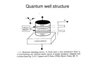
What is a quantum well? • A quantum well is similar to a potential well, the difference being that is only contains discrete energy values. [8] • Generally, a quantum well is formed when a thin layer of a narrow-gap semiconductor material lies between a thicker layer of wider-gap material. [1] • The size of the quantum wells are generally between 1 and 20 nm. [1] Example of a GaAs rectangular well [4]
The Behavior of Quantum Well Structures • Band gaps act as a barriers between the ground state bands and conduction bands, preventing electrons from reaching the conduction band unless they gain more energy. • Once an electron reaches the conduction band, the excess energy is released and the electron falls back to its ground state. • If the gaps are too wide for electrons to jump easily, thin semiconductors are placed in the gap area. • This allows for easy manipulation of the electrons and their energy. • The wells create narrow streams of energy making it more focused. [1]
More examples of quantum well structures Example of a parabolic quantum well [4] Second example of rectangular quantum well [7]
Commonly used materials and methods of quantum well fabrication • Some of the commonly used materials used to create quantum wells include: Gallium Arsenide between Aluminum Arsenide and Indium Gallium Nitride between Gallium Nitride. • There are two methods of fabrication which include: molecular beam epitaxy and chemical vapor deposition. [8]
Molecular Beam Epitaxy • Epitaxy means the growth of a film with a crystallographic relationship between substrate and the film. • Creating quantum wells like this is often expensive but highly accurate. • The process is often carried out in a vacuum and uses multiple alloys to grow the alloy films. [3] • Elements are heated until they are gaseous and then condense onto the wafer. • The term beam refers to the evaporated atoms that do not interact with each other until they reach the wafer. [6] Typical components and layout of the main chamber of MBE system [6]
Chemical Vapor Deposition • Similar to BME, but instead is a chemical process where the wafer is exposed to volatile precursors, which then react and decompose on the substrate to create the film. • A precursor is a chemical compound that takes part in the chemical reactions producing another chemical compound. [2] A chemical vapor deposition method using plasma [2]
Practical Uses of Quantum Well Structures • Quantum wells can be seen mostly in the making of diode lasers. [1] • These lasers include red lasers for DVDs and handheld laser pointers, infrared lasers for fiber optic transmitters, and blue lasers for Blu-ray players, etc… [7] • The Navy has recently demonstrated that a laser can be used to destroy surveillance drones. Video of Navy using a laser to take down a surveillance drone [5]
Summary and Conclusion • Quantum wells are potential wells with discrete energy values. • Quantum wells are formed using one of two methods: molecular beam epitaxy or chemical vapor deposition. • Quantum wells are seen mostly in the fabrication of laser diodes. • Quantum wells have lead to some very useful products in our society, i.e. Blu-ray lasers, DVD lasers, free electron lasers (medical purposes, military uses).
References • [1] Bates, Angie. "What Is a Quantum Well?" WiseGeek. Ed. Lauren Fritsky. Conjecture, n.d. Web. 28 Apr. 2013. <http://www.wisegeek.com/what-is-a-quantum-well.htm>. • Used to describe what a quantum well is, the behavior of a quantum well, and what they are used in. • [2] "Chemical Vapor Deposition." Wikipedia. Wikimedia Foundation, 21 Apr. 2013. Web. 28 Apr. 2013. <http://en.wikipedia.org/wiki/Chemical_vapor_deposition>. • Used to describe the CVD process. • [3] Christensen, Thomas M. "Physics of Thin Films." Molecular Beam Epitaxy. University of Colorado, Colorado Springs, 17 Mar. 2010. Web. 29 Apr. 2013. <http://www.uccs.edu/~tchriste/courses/PHYS549/549lectures/mbe.html>. • Used to explain the MBE process. • [4] Frensley, William R. "Quantum Wells." Quantum Wells. University of Texas, Dallas, 21 May 1995. Web. 28 Apr. 2013. <http://www.utdallas.edu/~frensley/technical/hetphys/node11.html>. • Used as a resource for rectangular and parabolic quantum well structure pictures.
References Cont. • [5] Knightskross. "U.S. Navy Laser Test Takes Down Drone." YouTube. YouTube, 08 Apr. 2013. Web. 28 Apr. 2013. <http://www.youtube.com/watch?v=l5qKSKsfUPM>. • Used for video of Navy laser destroying surveillance drone. • [6] "Molecular Beam Epitaxy." Wikipedia. Wikimedia Foundation, 21 Apr. 2013. Web. 28 Apr. 2013. <http://en.wikipedia.org/wiki/Molecular_beam_epitaxy>. • Used to describe the MBE process. • [7] Schubert, E. F. "Quantum Wells (QWs)." Rensselaer Polytechnic Institute, 2003. Web. 28 Apr. 2013. <http://www.ecse.rpi.edu/~schubert/Course-ECSE-6290%20SDM-2/1%20QWs%20MQWs%20and%20SLs.pdf>. • Used as a resource for a quantum well structure picture. • [8] "Quantum Well." Wikipedia. Wikimedia Foundation, 29 Mar. 2013. Web. 28 Apr. 2013. <http://en.wikipedia.org/wiki/Quantum_well>. • Used to describe some of the uses of quantum wells and what a quantum well is.
List of Five Key Concepts • Quantum wells are similar to potential wells but with discrete energy values. • Quantum wells are placed so electrons can jump from valence band to conduction band more easily. • Quantum wells create a more focused, narrow stream of energy. • Quantum wells are created using either molecular beam epitaxy or chemical vapor deposition. • Quantum wells are seen mostly in the fabrication of laser diodes.