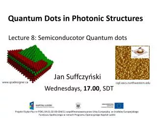
Quantum Dots in Photonic Structures
Lecture 8: Semiconducotor Quantum dots. Quantum Dots in Photonic Structures. Wednesdays , 17.00 , SDT. Jan Suffczyński. cqd.eecs.northwestern.edu. www.qcadesigner.ca. Projekt Fizyka Plus nr POKL.04.01.02-00-034/11 współfinansowany przez Unię Europejską ze środków Europejskiego

Quantum Dots in Photonic Structures
E N D
Presentation Transcript
Lecture 8: Semiconducotor Quantum dots Quantum Dots in PhotonicStructures Wednesdays, 17.00, SDT Jan Suffczyński cqd.eecs.northwestern.edu www.qcadesigner.ca Projekt Fizyka Plus nr POKL.04.01.02-00-034/11 współfinansowany przez Unię Europejską ze środków Europejskiego Funduszu Społecznego w ramach Programu Operacyjnego Kapitał Ludzki
Plan for today Reminder 2. Excitons in semiconductor quantum dots 3. Ordering in self-organized Quantum Dot system
Holes • Consider an insulator (or semiconductor) with a few electrons excited from the valence band into the conduction band • “Deficiency” of negative charge can be treated as a positive charge • Negativecurvature of the band negative hole effective mass
Semiconductor Quantum Well Confinement potential
ky kx nz ny kx nz nz nx ny Quantum Confinement inNanostructures Confinementin: 1 Direction: Quantum well (thin film) Two-dimensional excitons 2 Directions: Quantum wire One-dimensional excitons 3 Directions: Quantum dot Zero-dimensional excitons Each confinement direction converts a continuous k in a discrete quantum number n.
Confinedlevels in Quantum Wells Energy of confinedlevels GaAs/AlGaAs Quantum Well Decrease of the levelenergywhenwidth of the Quantum Welldecreased R. Dingle, Festkorperprobleme’1975
Confinedlevels in Quantum Dots Photoluminescence of GaAs/GaAlAs Quantum Dots QD as anartificial atom B. Piętka et al.
QD types and fabricationmethods • Goal: to engineer potential energy barriers to confine electrons in 3 dimensions • Basic types/methods • Colloidal chemistry • Electrostatic • Lithography • Epitaxy • Fluctuation • Self-organized • Patternedgrowth - „Defect” QDs
Photoluminescence spectra of GaN template on sapphire GaNgrown on 11-22 direction, CEA Valbonne • Anevidence for narrow, discreteemission lines!
„Defect” type quantum dots HRTEM, S. Kret, IF PAN
CubicGaNvs wurtziteGaN • Energy of emission (~3.25-3.45 eV) agreesresonably with anexpectation for cubicGaNinclusions in wurtziteGaN
Self-organized Semiconductor QDs • Number of atoms ~ 103 - 106 C. H. Li et al, APL’2005
Epitaxy: Self-Organized Growth Self-organized QDs through epitaxial growth strains • Stranski-Krastanov growth mode (use MBE, MOCVD) • Islands formed on wetting layer due to lattice mismatch (size ~10snm) • Disadvantage: size and shape fluctuations, strain, • Control island initiation • Induce local strain, grow on dislocation, vary growth conditions, combine with patterning Lattice-mismatchinduced islandgrowth
Semiconductor Quantum Dot Klimeck et al.
QD confinedelectronwavefunctions Klimeck et al.
InGaAsself-assembledQDs Calculatedconfined eh-pair energies forInAsassuming pyramidal shape Grundmann, Bimberg et al., TU Berlin
CdTeQDsqrowth – amorfous Te depositionmethod J. Kobak et al. GaAs:Si substrate F. Tinjod et al., APL (2003)
CdTeQDsqrowth – amorfous Te depositionmethod J. Kobak et al. ZnTe buffer 1000 nm GaAs:Si substrate F. Tinjod et al., APL (2003)
CdTeQDsqrowth – amorfous Te method ZnTe buffer 1000 nm GaAs:Si substrate CdTelayer F. Tinjod et al., APL (2003)
CdTeQDsqrowth – amorfous Te depositionmethod J. Kobak et al. amorphous Te ZnTe buffer 1000 nm GaAs:Si substrate CdTelayer F. Tinjod et al., APL (2003)
CdTeQDsqrowth – amorfous Te depositionmethod J. Kobak et al. amorphous Te QDs ZnTe buffer 1000 nm GaAs:Si substrate F. Tinjod et al., APL (2003)
CdTeQDsqrowth – amorfous Te depositionmethod J. Kobak et al. QDs ZnTe buffer 1000 nm GaAs:Si substrate F. Tinjod et al., APL (2003)
CdTeQDsqrowth – amorfous Te depositionmethod J. Kobak et al. ZnTe cap 100 nm ZnTe buffer 1000 nm GaAs:Si substrate F. Tinjod et al., APL (2003)
Control of CdTe/ZnTe QD densitywith the temperature of CdTedeposition PL intensity µPL 6 K 0 – 2 QDs 15 – 30 QDs 30 – 60 QDs 300 – 600 QDs 3 ML 80 – 160 QDs 500 – 1000 QDs 1900 2000 2100 2200 2300 2400 2500 Photon Energy (meV) J. Kobak et al., arXiv:1210.2946 (2012)
Control of CdTe/ZnTe QD density with the thickness of CdTelayer PL intensity T=334 oC µPL 6 K 1 ML 10 – 20 QDs 2 ML 100 – 200 QDs 3 ML 300 – 600 QDs 4 ML 500 – 1000 QDs 1900 2000 2100 2200 2300 2400 2500 Photon Energy (meV) J. Kobak et al., arXiv:1210.2946 (2012)
Control of CdTe/ZnTe QD density with the thickness of CdTelayer
Epitaxy: Patterned Growth • Growth on patterned substrates • Grow QDs in pyramid-shaped recesses • Recesses formed by selective ion etching • Disadvantage: density of QDs limited by mask pattern T. Fukui et al. GaAs tetrahedral quantum dot structures fabricated using selective area metal organic chemical vapor deposition. Appl. Phys. Lett. May, 1991
Exciton formation The absorption of photon by an interband transition in a semiconductor or insulator createsan electron in the conduction band and hole in the valence band. Eg
Exciton formation This oppositely charged particles attract each other though Coulomb interaction, and there may be the probability of the formation of neutral electron-hole pair called an Exciton.
Exciton formation Wannier-Mott excitons Frenkel exciton
Exciton – Bohr model Wannier-Mott excitons ModdifiedBohr model of the hydrogen atomapplies reduced mass bindingenergy dielectricconstant
Exciton bindingEnergy Ry(H) = 13.6 eV Binding Energy ofelectron in Hydrogen atom • Exciton compared to hydrogen atom: • largerratio of the effective masses • electron and hole are in medium with dielectric constant ranging between 10-30, • Smallerexciton binding energy For stability of Excitons binding energy must be higher than ∼ kBT
Exciton Bohr Diameter - bulk • The same size dot of different material may • not assure quantum confinement
Oscillatorstrength of the exciton recombinationconfined in QD J. Hours, P. Senellart, E. Peter, A. Cavanna, and J. Bloch, PHYSICAL REVIEW B (R)2005
Oscillatorstrength of the exciton recombinationconfined in QD
How to observeexcitons in Semiconductor Quantum Dots?
Spectroscopy of individual Quantum Dots Towardsdetector Laser beam Microscopeobjective Sample with QDs
Experimental setup Laser beam
Microscopeobjective Spatial resolution <1m) J. Jasny and J. Sepioł, Chem. Phys. Lett. 273, 439 1997.
QD exciton emission QDsensambleemission Individual QD emission spectrum
X X: Excitonic transitions in a quantum dot Exciton (X)
XX XX: Excitonic transitions in a quantum dot Biexciton (XX)
CX CX: Excitonic transitions in a quantum dot Charged exciton (X+ or X-)
Neutral exciton X X • Formed by: heavy hole and electron • Jz = ±3/2 • Jz = ±1/2 • 4 possiblespinstates of X Xdark X • Jz= -2 • Jz= -1 • Jz= +1 • Jz= +2
Fine structure of neutral exciton ( + )/ X δ1~0.1meV ( – )/ X Anisotropic exchange δ0~1meV Isotropic exchange ( + )/ δ2 ≈0 Xdark ( – )/