Download
1 / 29
330 likes | 757 Vues
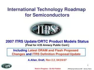
International Technology Roadmap for Semiconductors 2007 ITRS Update/ORTC Product Models Status [Final for 4/25 Annecy Public Conf.] A.Allan, Draft, Rev 2.2, 04/24/07. Including Latest DRAM and Flash Proposed Changes and ITRS Definition Proposal/Update.

E N D
International Technology Roadmap for Semiconductors 2007 ITRS Update/ORTC Product Models Status [Final for 4/25 Annecy Public Conf.] A.Allan, Draft, Rev 2.2, 04/24/07 Including Latest DRAM and Flash Proposed Changes and ITRS Definition Proposal/Update
[Updated Proposals and extend to 2022] ORTC Pre-Summary – 2007 Renewal [plus Area efficiency delayed year] • DRAM Model stagger-contacted M1 half-pitch unchanged from 2005 ITRS (3-year cycle* after 2004), however Bits/Chip shifted by one year; 6f2/2006-22 • MPU M1 stagger-contact half-pitch unchanged on a 2.5-year cycle* through 2010/45nm, then 3-year cycle*. • Flash Model un-contacted poly half-pitch Extended on 2-year cycle* to 2 years ahead of DRAM (contacted) in 2008, then 3-year cycle*. • Printed MPU/ASIC Gate Length is set by FEP and Litho TWGs ratio agreement, but Physical GL targets unchanged and on 3-year cycle* beginning 2005. • New 2007 Definitions added: • “Moore’s Law” (typically digital computing) Functional and Performance scaling is enabled by both “Geometrical” and also “Equivalent” scaling technologies • “Functional diversification” (typically non-digital sensing, interacting) system board-level migration/miniaturization is enabled by system-in-package and system-on-chip • Industry Technology Capacity (SICAS) [2Q06 published status] continues on a on 2-year cycle rate at the leading edge. • Total MOS Capacity (SICAS) is growing ~12% CAGR (SICAS), and 300mm Capacity Demand has ramped to 25% of Total MOS. • Historical unchanged chip size models are “connected” to Product scaling rate models, and include design factors, function size, and array efficiency targets • The average of the industry product “Moore’s Law” (2x/chip per 2 years) continues to be met throughout the latest 2007-2022 ITRS timeframe [* ITRS Cycle definition = time to .5x linear scaling every two cycle periods]
Comment From the 2006 Update Executive Summary: “…Overall, the 2006 ITRS Update represents a minor modification to the 2005 ITRS. The 2006 ITRS Update, consistent with the 2005 ITRS, removes the concept of “technology node” as the main pace setter for the IC industry. Users of the 2006 Update easily can determine specific numbers for DRAM metal half-pitch, NAND polysilicon half-pitch, or MPU and ASIC gate length, for example, to characterize the pace of that specific technology. The Overall Roadmap Technology Characteristics Tables and individual ITWG tables use these specific product timings to indicate the drivers for their requirements. For this purpose, the 2006 ITRS Update addresses an independent measure of the technology pace of DRAM, of MPU, and of Flash products….”Several tables have been corrected or updated, as clearly indicated in blue. It is also rather easy to identify where the changes have occurred as indicated by “IS” in the far left column of an updated table. This Overview document contains an Appendix of all tables, figures, or textual changes for the 2006 Update by chapter.It is important to remind the reader that it is the purpose of the ITRS documents to provide a reference of requirements, potential solutions, and their timing for the semiconductor industry. This objective has been accomplished by providing a forum for international discussion, cooperation, and agreement among the leading semiconductor manufacturers and the leading suppliers of equipment, materials, and software, as well as researchers from university, consortia, and government labs. The ITRS documents have become and remain a truly common reference for the entire semiconductor industry. Indeed, the cooperative efforts of the ITRS participants have fostered cooperation among international consortia, universities, and research institutions around the world. It is hoped that the 2006 ITRS Update will further contribute to fuel cooperative R&D investments so that the financial burden can be more uniformly shared by the whole industry. It is also hoped that the ITRS will continue to stimulate the fundamental elements that encourage innovation in individual companies.
ORTC Overview – 2007 Update ITRS - Update [changes to DRAM and Flash extend to 2022] • DRAM will not be standard TWG table technology trend header • 2007 ITRS Update DRAM 3-year cycle stagger-contacted Unchanged, • However, Bits/chip delayed 1Year; 6f2 2006-2022 • ORTC Table 1a,b - MPU/ASIC M1 Half-Pitch Trend Unchanged • Stagger-contacted, same as DRAM • 2.5-year Technology Cycle* (.5x/5yrs) • 180nm/2000; 90nm/2005; 45nm/2010(equal DRAM) • Then continue on a 3-year Technology Cycle*, equal to DRAM 2010-2020 • ORTC Table 1a,b - STRJ Flash Poly (Un-contacted dense lines) • 2-year Technology Cycle* (0.5x/4yrs) Extended to 2008 • 180nm/2000; 130nm/2002; 90nm/2004; 65nm/2006; 45nm pull-in to 2008 • Then return to 3-year Technology Cycle* 2 years ahead of DRAM ’08-’22 • ORTC Table 1a,b – MPU/ASIC Printed Gate Length per FEP and Litho TWG ratio relationship to Final Physical Gate Length - 2005 ITRS target for (3-year cycle* after 2005 remains Unchanged at present. • TWG table Product-specific technology trend driver header items will be added in 2007 to individual TWG tables from ORTC Table 1a&b • Chip Size Models will be connected to latest DRAM and Flash proposals and Function Size [Logic Gate; SRAM Cell; Dram Cell; Flash Cell (SLC, MLC)] • Functions/Chip [Flash; DRAM; High Performance (hp) MPU; Cost Perf. (cp) MPU] • Chip Size [hp MPU; cp MPU; DRAM; Flash] *Note: Cycle = time to 0.5x linear scaling every two cycle periods ~ 0.71x/ cycle
2007 Definition of the Half Pitch - unchanged [No single-product “node” designation; DRAM half-pitch still litho driver; however, other product technology trends may be drivers on individual TWG tables] FLASH Poly Silicon ½ Pitch = Flash Poly Pitch/2 DRAM ½ Pitch = DRAM Metal Pitch/2 MPU/ASIC M1 ½ Pitch = MPU/ASIC M1 Pitch/2 • Poly • Pitch • Metal • Pitch 8-16 Lines Typical flash Un-contacted Poly Typical DRAM/MPU/ASIC Metal Bit Line Source: 2005 ITRS - Exec. Summary Fig 2
2007 - Unchanged Fig 3 Production Ramp-up Model and Technology Cycle Timing 100M 200K Development Production 10M 20K 1M 2K Alpha Tool Beta Tool Production Tool Volume (Parts/Month) 100K Volume (Wafers/Month) 200 First Two Companies Reaching Production 10K 20 First Conf. Papers 1K 2 0 12 24 -24 -12 Months Source: 2005 ITRS - Exec. Summary Fig 3
2007 (’07-’22) ITRS Technology Trends DRAM M1 Half-Pitch : 3-year cycle Update 2022 11 2007 2001 2001 2003 2003 2005 2005 2006 2008 2009 2012 2015 2018 2020 14 2000 [Actual] 2000 [Actual] 2002 [Actual] 2002 [Actual] 2004 2004 2010 2013 2016 2019 65 90 90 45 32 22 16 130 130 180 180 151 107 80 71 57 50 2-Year Technology Cycle [‘98-’04] Year of Production Year of Production Year of Production 2005 ITRS Flash Poly Half-Pitch Technology: 2.0-year cycle until 2yrsahead of DRAM @ 45nm/’08 3-Year Technology Cycle 3-Year Technology Cycle 2008 2010 2013 2016 2019 2020 2022 10 2006 2009 2012 2015 2018 Technology - Contacted M1 H-P (nm) Technology - Uncontacted Poly H-P (nm) Technology - Contacted M1 H-P (nm) 13 2001 2002 2003 2004 2006 2007 2008 2009 2012 2015 2018 2020 65 45 32 22 16 57 151 107 76 50 2010 2013 2016 2019 ’07‘08’09 ’10’11’14 ‘17‘20 IS: 53 45 40 36 3222 16 11 45 32 22 16 180 [130] 90 [ 65] 157 136 119 103 78 68 59 52 3-2-Yr Cycle] 2-Year Technology Cycle [’98-’06 ] 2.5-Year Technology Cycle 3-Year Technology Cycle 2005 ITRS MPU M1 Half-Pitch Technology: 2.5-year cycle; then equal DRAM @45nm/2010 2022 11 2000 [July’02] 2005 [July’08] 14
Figure 8 ITRS Product Technology Trends – [+ Update Flash] Fig 7&8 Simplified – Option 1 [DRAM &, MPU Unchanged; plus extend all to 2022] After 1998 .71X/2YR MPU M1 .71X/2.5YR Before 1998 .71X/3YR MPU & DRAM M1 & Flash Poly .71X/3YR Flash Poly .71X/2YR Flash 2YR Extended Gate Length .71X/3YR GLpr IS = 1.6818 x GLph Nanotechnology (<100nm) Era Begins -1999 2025 2007 - 2022 ITRS Range
2007 ITRS Executive Summary Fig 5 [under review/revision for 2007] [2007 – add Definitions; Update Graphic] Traditional ORTC Models Functional Diversification (More than Moore) [Geometrical & Equivalent scaling] Scaling (More Moore) Source: 2005 ITRS Document online at: http://www.itrs.net/Links/2005ITRS/Home2005.htm Continuing SoC and SIP: Higher Value Systems
Baseline CMOS HV Power Sensors, Actuators Bio-chips, Fluidics Memory RF Passives “More Moore” “More than Moore” Computing & Data Storage Sense, interact, Empower Heterogeneous Integration System on Chip (SOC) and System In Package (SIP) Source: ITRS, European Nanoelectronics Initiative Advisory Council (ENIAC) 2007 ITRS “Moore’s Law and More” Definition Graphic Proposal
2007 ITRS Definitions Proposal: “More Moore” and “More than Moore” • Scaling (“More Moore”) • Geometrical (constant field) Scaling refers to the continued shrinking of horizontal and vertical physical feature sizes of the on-chip logic and memory storage functions in order to improve density (cost per function reduction) and performance (speed, power) and reliability values to the applications and end customers. • Equivalent Scaling which occurs in conjunction with, and also enables, continued Geometrical Scaling, refers to 3-dimensional device structure (“Design Factor”) Improvements plus other non-geometrical process techniques and new materials that affect the electrical performance of the chip. • Functional Diversification (“More than Moore”) • Functional Diversificationrefers to the incorporation into devices of functionalities that do not necessarily scale according to "Moore's Law," but provide additional value to the end customer in different ways. The "More-than-Moore" approach typically allows for the non-digital functionalities (e.g. RF communication, power control, passive components, sensors, actuators) to migrate from the system board-level into a particular package-level (SiP) or chip-level (SoC) potential solution.
metal poly high k SiON gate stack bulk electrostatic control planar 3D MuGFET MuCFET FDSOI PDSOI + high µmaterials + substrate engineering stressors [ ITRS DRAM/MPU Timing: 2007/7.5 2010 2013 2016 ] Source: ITRS, European Nanoelectronics Initiative Advisory Council (ENIAC) 65nm 45nm 32nm 22nm PIDS/FEP - Simplified Transistor Roadmap[Examples of “Equivalent Scaling” from ITRS PIDS/FEP TWGs]
[Back to ORTC 2007 Renewal Update] • ITRS Technology Demand Tracking [SICAS] • ITRS Function Size Models • ITRS Functions/Chip Models • ITRS Chip Size Models • Summary
Fig 4 2005 ITRS Technology Cycle Timing Compared to Actual Wafer Production TechnologyCapacity Distribution [2007–need 3Q07 Update] ITRS Technology Cycle 10 W.P.C.= Total Worldwide Wafer Production Capacity(Relative Value *) Source: SICAS** W.P.C W.P.C W.P.C W.P.C W.P.C W.P.C W.P.C W.P.C W.P.C >0.7mm 720nm SIA/SICAS Data**: 1-yr delay from ITRS Cycle Timing to 25% of MOS IC Capacity 0.7-0.4mm 510nm 1 Feature Size (Half Pitch) (mm) 0.4-0.3mm 360nm (Feature Size of Reported Technology Capacity of SICAS Participants) <0.4mm <0.4mm <0.3mm <0.3mm 0.3- 0.2mm <0.2mm <0.2mm 255nm <0.16mm <0.16mm 0.1 <0.12mm 0.2- 0.16mm 180nm = 2003/04 ITRS DRAM Contacted M1 Half-Pitch Actual = 2005 ITRS DRAM Contacted M1 Half-Pitch Target 0.16-.12mm 127nm 3-Year Cycle 2-Year Cycle 3-Year Cycle 0.01 1997 1998 1999 2000 2001 2002 2003 2004 2005 2006 2007 <0.12mm 90nm Source: 2005 ITRS - Exec. Summary Fig 4 Year * Note: The wafer production capacity data are plotted from the SICAS* 4Q data for each year, except 2Q data for 2005. The area of each of the production capacity bars corresponds to the relative share of the Total MOS IC production start silicon area for that range of the feature size (y-axis). Data is based upon capacity if fully utilized. ** Source: The data for the graphical analysis were supplied by the Semiconductor Industry Association (SIA) from their Semiconductor Industry Capacity Statistics (SICAS). The SICAS data is collected from worldwide semiconductor manufacturers (estimated >90% of Total MOS Capacity) and published by the Semiconductor Industry Association (SIA), as of July, 2005. The detailed data are available to the public online at the SIA website, http://www.sia-online.org/pre_stat.cfm .
[2007–need 2Q07 Update] 0.71x 0.85 to 0.72u to.60u SICAS 90nm Capacity Tracking Kickoff – 2Q06 Update 0.60 to 0.51u to.42u 0.42 to 0.36u to.30u 0.30 to 0.25u to.21u n-2 0.21 to 0.18u to.15u n-1 0.15 to 0.13u to.11u n 0.11 to 0.090u to 0.075u Next TBD?: 20% 1Q07? (2yr Cycle) 1Q08? 3yr Cycle <0.075 to 0.065u to.053u ~32% of Total MOS n+1 [available 2Q07] Technology Demand 2-year Cycle Continues! 2-yrs to >20% of Total MOS for 0.71x Technology Reduction Cycle Source: SIA/SICAS Report: www.sia-online.org/pre_statistics.cfm
SICAS 300m Capacity Tracking – 2Q06 Update [2007–need 2Q07 Update] 1Q97-1Q06 Total MOS 9.1% CAGR [Total MOS only – 8” Equivalent] 12.0% YoY Wafer Starts per Week (1K) 2004 – Happy 10th Anniv. SICAS! 1Q97-1Q06 200mm 15.3% CAGR 11.6% CAGR 17.4% YoY 43.0% YoY 821.4 [100%] 93.1% YoY 728.2 [100%] 362.7 [44%] 277.4 [38%] 1Q 97 4Q 97 1Q 07 2Q 07 3Q 07 4Q 07 3Q 07 4Q 07 1997 2003 2004 2005 2005 2006 2006 2007 2Q06: 300mm = 25% of Total MOS 200mm = 62% of Total MOS <200mm = 14% of Total MOS 11 years intro-intro Wafer Generation 200mm/1Q97 SICAS Tracking Begins (7yrs after Intro) 300mm/1Q04 (3yrs after Intro) Source: SIA/SICAS Report: www.sia-online.org
Figure 9 ITRS Product Function Size – [Plus Updates] Fig xx Simplified [changes to DRAM and Flash extend to 2022] Logic Gate: NO Design Area Factor Improvement (Only Scaling) SRAM: Gradual Design Area Factor Improvement DRAM: 6f2 Last Design Area Factor Improvement DRAM 6f2 Pull-in to ‘06 (@ 2 MLC bits/physical cell area) Flash 2YR Extended Flash: 4f2 Design Physical Area Factor Improvement Flash: (MLC @ 2 bits/cell = 2f2 Equivalent Area Factor) Flash 4 bits/cell 1f2 Begin 2010 Note for Flash: SLC = Single-Level-Cell Size MLC = Multi-Level-Cell (Electrical Equivalent) Cell Size 2007 - 2022 ITRS Range
Past Future Chip Size Trends – 2005 ITRS Functions/Chip Model – Needs Update [2007 - extend to 2022] (@Volume Production, Affordable Chip Size**) ** Affordable Production Chip Size Targets: DRAM, Flash < 145mm2 hp MPU < 310mm2 cp MPU < 140mm2 Average Industry 1970-2020 “Moore’s Law” 2x Functions/chip Per 2 years MPU ahead or = “Moore’s Law” 2x Xstors/chip Per 2 years Thru 2010 ** Example Chip Size Targets: 1.1Gt P07h MPU @ intro in 2004/620mm2 @ prod in 2007/310mm2 ** Example Chip Size Targets: 0.39Gt P07c MPU @ intro in 2004/280mm2 @ prod in 2007/140mm2 2005 - 2020 ITRS Range
Figure 10 ITRS Product Functions per Chip DRAM & Flash Update [plus extend to 2022] Flash MLC 4 bits/chip 2010 Average Industry 1970-2020 “Moore’s Law” 2x Functions/chip Per 2 years 2022 Flash SLC Bits/chip for 1-year technology Pull-in update DRAM Bits/chip one-year bits/chip generation Delay; 2025 Past Future 2007 - 2022 ITRS Range
Chip Size Trends – 2005 ITRS DRAM Model – Update 2007 - extend to 2022; plus: DRAM chip size shrinks Due to one-year bits/chip generation Delay; 6.0 Past Future 2007 - 2022 ITRS Range
Chip Size Trends – 2005 ITRS Flash Model - Update 2005: [2007 - extend to 2022] Pull-in 1yr & Shrink 6.0 2007 - 2022 ITRS Range Past Future
[2007 - extend to 2022] Chip Size Trends – 2005 ITRS MPU Model - unchanged p25h p25c P22h 35.4Bt P22c 12.4Bt 2007 - 2022 ITRS Range Past Future
[Updated Proposals and extend to 2022] ORTC Pre-Summary – 2007 Renewal [plus Area efficiency delayed year] • DRAM Model stagger-contacted M1 half-pitch unchanged from 2005 ITRS (3-year cycle* after 2004), however Bits/Chip shifted by one year; 6f2/2006-22 • MPU M1 stagger-contact half-pitch unchanged on a 2.5-year cycle* through 2010/45nm, then 3-year cycle*. • Flash Model un-contacted poly half-pitch Extended on 2-year cycle* to 2 years ahead of DRAM (contacted) in 2008, then 3-year cycle*. • Printed MPU/ASIC Gate Length is set by FEP and Litho TWGs ratio agreement, but Physical GL targets unchanged and on 3-year cycle* beginning 2005. • New 2007 Definitions added: • “Moore’s Law” (typically digital computing) Functional and Performance scaling is enabled by both “Geometrical” and also “Equivalent” scaling technologies • “Functional diversification” (typically non-digital sensing, interacting) system board-level migration/miniaturization is enabled by system-in-package and system-on-chip • Industry Technology Capacity (SICAS) [2Q06 published status] continues on a on 2-year cycle rate at the leading edge. • Total MOS Capacity (SICAS) is growing ~12% CAGR (SICAS), and 300mm Capacity Demand has ramped to 25% of Total MOS. • Historical unchanged chip size models are “connected” to Product scaling rate models, and include design factors, function size, and array efficiency targets • The average of the industry product “Moore’s Law” (2x/chip per 2 years) continues to be met throughout the latest 2007-2022 ITRS timeframe [* ITRS Cycle definition = time to .5x linear scaling every two cycle periods]
Note: ITRS Table Colorization Code Reference unchanged: Backup Source: 2005 ITRS Documents online at: http://www.itrs.net/Links/2005ITRS/Home2005.htm
IRC “Moore’s Law and Moore” Definition, Rev5, 04/24/07 [Glossary Proposal for 2007 ITRS Renewal] 1) Scaling (“More Moore”) 1a) Geometrical (constant field) Scaling refers to the continued shrinking of horizontal and vertical physical feature sizes of the on-chip logic and memory storage functions in order to improve density (cost per function reduction) and performance (speed, power) and reliability values to the applications and end customers. Examples (not exhaustive) are: a) horizontal half-pitch feature size (f^2) for density/cost; b) gate insulator thickness for speed and power performance; c) gate length for speed performance. Slowing of geometrical scaling reduces the rate at which the end applications and customers receive value benefits, requiring new “equivalent scaling” material and/or gate enhancements.1b) Equivalent Scaling which occurs in conjunction with, and also enables, continued Geometrical Scaling, refers to 3-dimensional device structure (“Design Factor”) Improvements plus other non-geometrical process techniques and new materials that affect the electrical performance of the chip. Examples (not exhaustive) are: a) horizontal or vertical function design factor (i.e. 3-dimensional capacitor and transistor designs); b) strained silicon in the transistor gate; c) flash memory electrical multi-bit-cell; d) high-K capacitor material for enhanced DRAM storage effectiveness; e) high-K transistor gate material substitutes for insulator thickness scaling; f) low-K chip-level interconnect material; and g) Packaging low-K interconnect materials (as this is required by point f above). Electrical equivalent scaling can enhance the value benefits of geometrical scaling. The objective of both geometrical (density) and equivalent scaling (including power and performance tradeoffs and extensions) is to sustain the CMOS shrinking as described by the classical "Moore's Law" (affordable on-chip doubling of functionality every two years) . 2) Functional Diversification (“More than Moore”) Functional Diversification refersto the incorporation into devices of functionalities that do not necessarily scale according to "Moore's Law," but provide additional value to the end customer in different ways. The "More-than-Moore" approach typically allows for the non-digital functionalities (e.g. RF communication, power control, passive components, sensors, actuators) to migrate from the system board-level into a particular package-level (SiP) or chip-level (SoC) potential solution. Other Examples (not exhaustive) are: a) on-chip logic plus software power management; b) stacked chips with through-vias for board-level density and power; c) diverse Specialized Functionality such as AMS/RF, Image Sensors, Sensors/Actuators (including MEMS), Embedded Passives, etc.; and d) Other possible packaging issues associated with SIP and SOP, etc.
2006 Update Executive Overview [delivered to Taiwan Press, 12/05/05]The International Technology Roadmap for Semiconductors (ITRS) is the result of a worldwide consensus-building process. This document predicts the main trends in the semiconductor industry spanning across 15 years into the future. The participation of experts from Europe, Japan, Korea, and Taiwan as well as the U.S.A. ensures that the ITRS is a valid source of guidance for the semiconductor industry as we strive to extend the historical advancement of semiconductor technology and the worldwide integrated circuit (IC) market. These five regions jointly sponsor the ITRS.The Semiconductor Industry Association (SIA) coordinated the first efforts of producing what was originally TheNational Technology Roadmap for Semiconductors (NTRS). The semiconductor industry became a global industry in the 1990s, as many semiconductor chip manufacturers established manufacturing or assembly facilities in multiple regions of the world. This realization led to the creation of the International Technology Roadmap for Semiconductors in the late 90s. The invitation to cooperate on the ITRS was extended by the SIA at the World Semiconductor Council in April 1998 to Europe, Japan, Korea, and Taiwan. Since then, full revisions of the ITRS were produced in 1999, 2001, 2003 and 2005; ITRS updates were produced in the even-numbered years (2000, 2002, and 2004).The ITRS process is an ongoing event. The industry is dynamic—continually innovating; introducing new products; and achieving solutions. To keep the ITRS information as current as possible with this dynamic industry environment, during each year following an edition such as the 2005 ITRS, the roadmap information is reviewed. Data adjustments, corrections, and new information items are agreed to among the ITWG members and by soliciting public feedback during the annual ITRS Summer Conference in San Francisco. For the 2006 ITRS Update effort, all the ITRS tables were reviewed. If necessary, data and notations were updated to match industry advancements.
2006 Update Executive Overview (continued)Overall, the 2006 ITRS Update represents a minor modification to the 2005 ITRS. The 2006 ITRS Update, consistent with the 2005 ITRS, removes the concept of “technology node” as the main pace setter for the IC industry. Users of the 2006 Update easily can determine specific numbers for DRAM metal half-pitch, NAND polysilicon half-pitch, or MPU and ASIC gate length, for example, to characterize the pace of that specific technology. The Overall Roadmap Technology Characteristics Tables and individual ITWG tables use these specific product timings to indicate the drivers for their requirements. For this purpose, the 2006 ITRS Update addresses an independent measure of the technology pace of DRAM, of MPU, and of Flash products.Several tables have been corrected or updated, as clearly indicated in blue. It is also rather easy to identify where the changes have occurred as indicated by “IS” in the far left column of an updated table. This Overview document contains an Appendix of all tables, figures, or textual changes for the 2006 Update by chapter.It is important to remind the reader that it is the purpose of the ITRS documents to provide a reference of requirements, potential solutions, and their timing for the semiconductor industry. This objective has been accomplished by providing a forum for international discussion, cooperation, and agreement among the leading semiconductor manufacturers and the leading suppliers of equipment, materials, and software, as well as researchers from university, consortia, and government labs. The ITRS documents have become and remain a truly common reference for the entire semiconductor industry. Indeed, the cooperative efforts of the ITRS participants have fostered cooperation among international consortia, universities, and research institutions around the world. It is hoped that the 2006 ITRS Update will further contribute to fuel cooperative R&D investments so that the financial burden can be more uniformly shared by the whole industry. It is also hoped that the ITRS will continue to stimulate the fundamental elements that encourage innovation in individual companies.
[2007 - extend to 2022] 2006 ITRS Update - Overall Roadmap Technology Characteristics Summary [page 1 of 2] The International Technology Roadmap for Semiconductors (ITRS) Overall Roadmap Technology Characteristics (ORTC) section provides both originating guidance from ORTC Product Models and also consolidates items from other ITRS Technology Working Group (TWG) tables. Table 1a-h Product Generations (DRAM, Flash, MPU/ASIC) and Chip Size Model Technology Trends —There are no changes from the 2005 ORTC Technology Trend and Product Models, and there are also no changes to the 2005 Product Performance Models provided by the Design TWG. As a result, the ORTC Tables 1a-i, which are sourced from those models, remain unchanged. There are some corrections made to the line item labels: 1) various cell area and transistor area labels, which were incorrectly labeled as “mm2” in the 2005 tables, instead of “um2”; and 2) Flash Memory bits per cm2 labeled “Gbits/cm2” (Giga-bits/ cm2) rather than “Bits/cm2.” The remaining changes to ORTC tables for the 2006 Update are derived from corresponding changes to TWG tables, which are used as the various source line items for consolidation in the ORTC. A review of these TWG-related ORTC Tables is included below. Table 2a&b Lithographic-Field and Wafer-Size Trends —Lithography field size trends are unchanged. Wafer generation targets (450mm target to begin in 2012 on 11-year cycle) remain unchanged by the International Roadmap Committee (IRC). It is important to note that dialogue is underway between semiconductor manufacturers and suppliers to assess standards and productivity improvement options on 300mm and 450mm generations. Economic analysis of option scenarios is also underway to examine the required R&D cost, benefits, return-on-investment, and funding mechanism analysis and proposals. Table 3a&b Performance of Packaged Chips: Number of Pads and Pins —Internal chip pad counts for both I/O and power and ground remain unchanged (2:1 ratio I/O-to-power/ground for high-performance MPU; 1:1 ratio for high-performance ASIC). After assessment of the progress in the back-end assembly and packaging industry, the Assembly and Packaging (A&P) TWG increased their numerical targets and trends for the maximum pin counts, increasing pressure on future packaging costs. Table 4a&b Performance and Package Chips: Pads, Cost —The A&P TWG increased the area array flip chip pad spacing targets by 10–20%. The two-row staggered-pitch targets have increased 10–20% in the near termand the three-row staggered-pitch targets have increased 10–50% in the near term. Both pitch targets remain unchanged in the long term. Cost-per-pin targetsare adjusted by the A&P TWG, to reflect estimates and response to cost challenges.
[2007 - extend to 2022] 2006 ITRS Update - Overall Roadmap Technology Characteristics Summary [continued page 2 of 2] Table 4c&d Performance and Package Chips: Frequency On-chip Wiring Levels —The A&P TWG adjusted the chip-to-board (off-chip) frequency targets in the 2011–2020 range to remain below the Design/Process Integration (PIDS) targets for on-chip frequency. The Design/PIDS targets for on-chip frequency remain unchanged in the 2006 Update. The Interconnect TWG leaves the number of on-chip wiring levels unchanged. Table 5a&b Electrical Defects —The MPU and DRAM defect targets are adjusted by the Yield Enhancement TWG to reflect their new 2006 Update models and trends, in which both random defects/cm2 and the number of mask levels have leveled off through 2020 at smaller long range targets. Table 6a&b Power Supply and Power Dissipation —There are no changes to the PIDS TWG MPU and DRAM targets for voltage. The A&P TWG kept the maximum power per square centimeter targets unchanged through 2018. The 2019 and 2020 targets, which increased in the 2005 table, are constant in the update table. The maximum Watts (calculated by the ORTC table for specific product maximum production start chip sizes) are also now constant targets in 2019 and 2020. Table 7a&b Cost —The “tops-down” semiconductor market driver models for cost-per-function remain unchanged for the the 2006 Update. The Cost table targets for both memory and logic represent the need to preserve the historical economic semiconductor device productivity trend for continuous reduction of the cost-per-function by -29% compound annual reduction rate (CARR) throughout the roadmap timeframe. Preserving this cost-per-function productivity trend in view of increasing packaging costs, plus the slowing of product function densities due to slower technology cycles (three-year versus two-year) and design factor improvements, represent the over-arching economic grand challenge for the industry.