Download
1 / 3
40 likes | 271 Vues
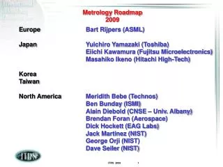
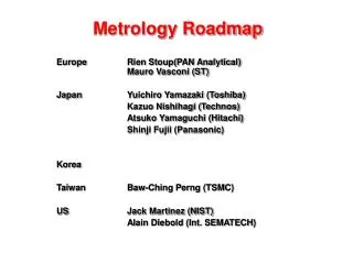
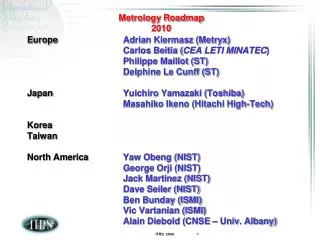
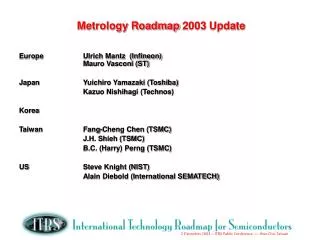
International Technology Roadmap for Semiconductors Metrology Roadmap 2012. Metrology Technical Working Group. Metrology Roadmap 2012 Spring attendance. Europe Carlos Beitia ( CEA LETI MINATEC ) Philippe Maillot (ST) Japan Masahiko Ikeno (Hitachi High-Tech) Korea Taiwan

E N D
International Technology Roadmap for SemiconductorsMetrology Roadmap2012 Metrology Technical Working Group
Metrology Roadmap 2012Spring attendance Europe Carlos Beitia (CEA LETI MINATEC) Philippe Maillot (ST) Japan Masahiko Ikeno (Hitachi High-Tech) Korea Taiwan North America Yaw Obeng (NIST) Ben Bunday (SEMATECH) Alain Diebold (CNSE)
Metrology Summary 3D Metrology • Litho • Metrology will update its DP tables • Working on 3D Measurement Tables • FEP • USJ Metrology Gap (profile and dose) requested Info • Defects in new channel materials Ge and III-V ‘s • What do Fins really look like what CD do we measure • Add Fin CD requirements to Litho Met tables • Interconnect • Void Characterization now R&D • Thermomechanical properties of patterns • K values of patterned films • ERD-ERM • Contact Resistance Measurement Gap • Work with ERM on e-Workshop on electrical Characterization • ES&H • Start coordination of ES&H measurements From Dick James – Chip Works SST Blog CVD Graphene F. Nelson CNSE