Metrology Roadmap 4 - 05
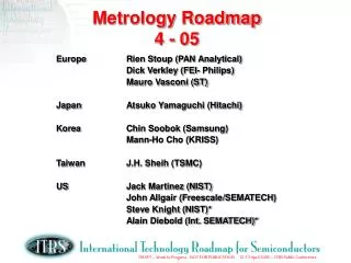
Metrology Roadmap 4 - 05. Europe Rien Stoup (PAN Analytical) Dick Verkley (FEI- Philips) Mauro Vasconi (ST) Japan Atsuko Yamaguchi (Hitachi) Korea Chin Soobok (Samsung) Mann-Ho Cho (KRISS) Taiwan J.H. Sheih (TSMC) US Jack Martinez (NIST)

Metrology Roadmap 4 - 05
E N D
Presentation Transcript
Metrology Roadmap4 - 05 Europe Rien Stoup (PAN Analytical) Dick Verkley (FEI- Philips) Mauro Vasconi (ST) Japan Atsuko Yamaguchi (Hitachi) Korea Chin Soobok (Samsung) Mann-Ho Cho (KRISS) Taiwan J.H. Sheih (TSMC) US Jack Martinez (NIST) John Allgair (Freescale/SEMATECH) Steve Knight (NIST)* Alain Diebold (Int. SEMATECH)*
AGENDA • 2005 ITRS Changes and Activities • Lithography Metrology • FEP Metrology • Interconnect Metrology • Key Challenges
Transistor Evolution Beyond CMOS Future 15 years Non-classical CMOS Tomorrow Molecular Switches ? Nanowire Transistor ? Today 90 nm Node CMOS pMOS FINFET New Materials Strain Enhanced Mobility
Nanotransistors – The Future Short Long Channel Behavior Idsat ( 1/Lg ) ( CarrierMobility ) ( 1/EOT ) ? Nano Transistors Idsat ~ W Cox (VG – VT) sat C dependence A = Lg x W Dopant Conc. = Cload VDD / Idsat
New Business • Established link with Emerging Research Materials group of ERD • ERM to report requirements • Metrology Reports Methods and Discussion • Provided update on aberration corrected TEM and 3D TEM developments • Awaiting changes in Process Tolerance for Gate CD
Changes to Litho CD Metrology ITRS July Presentation by Dan Wack – KLA-Tencor Scatterometry to at least the 45 nm Node Bryan Rice (Intel), SPIE, 2004 CD-SEM and Scatterometry can reach 32 nm Node w/improvement – impact of SOI not tested 45 nm contact Holes 16 nm Lines -176 nm Pitch
Japan ITRS TWG Input LWR as a Function of L L above 2 m is really CD variation 2mm CD variation Experiments 3s (nm) Simulation LWR increase becomes negligible at L=2mm Average LWR Inspection-area height L (nm) Confirmed by ... Experiments & Simulation L value works for many resists as well as ADI, resist trim, and after etch
Trend: Sidewall Control will become more ImportantLine Edge Roughness impacts Interconnect Resistance and Line Width Roughness impacts Transistor Leakage Current p=0(complete diffuse scattering) 5 Measured Cu resistivity without Barrier Metal p=0.3 4 Updated(May2004) ρ(Al):2.74μΩcm 3 Resistivity(μΩcm) 2 p=0.5 1 0 0 100 200 300 400 500 Wire width(nm)
LER and LWRreported as RMS values integrated over the frequency range specified below • Measure LER and LWR = for reliability all spatial wavelengths between 1 micron to 20 nm taken over a 2 micron length with a spacing of 10 nm. • LER: For monitoring Interconnect specular scattering – measure from 34 nm to twice the smallest interval using the smallest possible interval. Measure sidewall after barrier metal dep.
Overlay Metrology • Issues are with the Overlay Targets • Need better correlation between overlay target and device performance • Current roadmap suggests that overlay is in good shape because precision for box – in – box targets meets ITRS guidelines • Step and Scan Litho Exposure tools contribute errors not measured by scribe line targets • Across die overlay issues are not captured by box –in – box target data analysis • 2005 rewrite will capture these issues
FEP Metrology:Increasing Emphasis on Areas beyond High k • Increase in Mobility by using local stressing of transistors – Call for stress metrology by FEP • Metal Gates increasingly important • New transistor designs are already past R and into D. Example: FIN-FETs require metrology • Strained SOI, GeOI considered longer term substrates • Crystal Defect mapping including on patterned wafers metrology requirement for new substrates • Mobility measurements are key
Stress Measurement from transistor to wafer Nano-Raman and CBED Transistor Level Stress Micro-Raman, XRD Micro-Area Level Stress Die level flatness Laser Interferometry New Interferometry Method Die Level Stress Wafer Bow Laser Interferometry, New Interferometry
Trend : Use Modeling to connect what you can measure with what you need to know Example: Metrology of Strained Channel Devices MD Giles, et. al., VLSI Symposium 2004
2005 Interconnect Activities • Porous low k is being overshadowed by the need to lower k value of barrier layer and etch stops for 45/32 nm node. • Long term solution for interconnect is ambiguous.
New Comments on Interconnect Metrology • 3D CD especially Sidewall Roughness for trench/via are critical needs • In Process Development, LER is an important figure of merit for sidewall and AFM can give sidewall/via roughness vs depth as well as trench CD and profiles which provide important control for etch processes • Need metrology for thickness and uniformity for hard mask above low after CMP – how is erosion pattern dependent
ERD and ERMPremise: Aberration corrected TEM/STEM needed for nano-electronics • Latest TEM and STEM results show improved imaging for sub 0.1 nm beams. • We have not reached the limit where improving beam diameter does not improve imaging • Nanowires and nanotubes serve as ideal systems to test theoretical and experimental understanding of beam propagation and image formation. - reduced stresses and amorphous films on the surface
Concept Proven : Aberration Correction STEM – Batson, Dellby, and Krivanek, Nature 418, 617 (2002) Si(110) HR-TEM – Jai, Lentzen, and Urban, Microsc. Microanal. 10, 174, 2004. SrTiO3 Before After
Conclusions • CD Measurement improvements show a path to the 32 nm Node • Propose definition for LWR and including LER • Transistor channel engineering requires Stress and Mobility Measurement • Interconnect requires Sidewall Measurements for barrier/seed and low trench
Acknowledgements • David Bell and his 2003 M&M paper on nanowire TEM • Christian Kiselowski • Dave Muller • Steve Pennycook • Suzanne Stemmer
Why measure CD for NanoTransistors = Cload VDD / Idsat 1. CD impacts Capacitance C A = Lg x W Dopant Conc. 2. CD impacts Threshold Voltage Likharev has shown that below 10 nm CD, Threshold Voltage is very sensitive to CD At CD = 5 nm Process range is 0.2 nm ~ 1 atom
Red moves back in? for Litho Metrology Technology Requirements
w 2q 2005 Potential Solution Assessments • Conflicting Reports on high keV CD-SEM Damage • Impact of Metal Gate on CD-SEM and Scatterometry – Metal Dependent • Impact of Gate thickness on CD Measurement for end of roadmap • New Method identified as potential solution – CD-SAXS (NIST Wen-li Wu)
FEP Metrology Questions • FINFET Metrology needs? • Doping • corner rounding makes FIN fully depleted with thicker FIN • Gate Dielectric Thickness • Timing schedule is ?? 2005 • FIB cross-section accuracy issues. • Particles on 450 mm wafer • 1mm edge exclusion • Local Strain • High k Gate stack (EOT, k, thickness) • SOI/BOX • Gate workfunction
High Volume ICs use CMOS w/ Locally Strained SiStrained Si substrates not used PMOS Compressive Strain increased hole mobility 45 nm NMOS Tensile Stress SiN Layer increased electron mobility From T. Ghani, et. al., IEDM 2003, p 978. Courtesy Intel
Gaps in Interconnect Metrology • VOID Detection in Copper vias & lines now based on 1/10 via diameter • Quality of Barrier/Seed on sidewalls • Killer Pore Detection in Low k • Non destructive metrology for adhesion and (eff) (at operating freq.) for patterned wafers