Metrology Roadmap
Metrology Roadmap. Europe Rien Stoup(PAN Analytical) Mauro Vasconi (ST) Japan Yuichiro Yamazaki (Toshiba) Kazuo Nishihagi (Technos) Atsuko Yamaguchi (Hitachi) Shinji Fujii (Panasonic) Korea Taiwan Baw-Ching Perng (TSMC) US Jack Martinez (NIST)
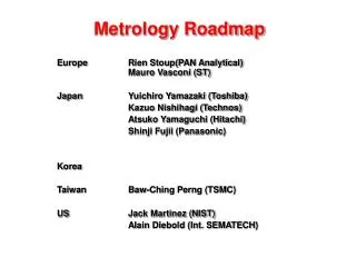

Metrology Roadmap
E N D
Presentation Transcript
Metrology Roadmap Europe Rien Stoup(PAN Analytical) Mauro Vasconi (ST) Japan Yuichiro Yamazaki (Toshiba) Kazuo Nishihagi (Technos) Atsuko Yamaguchi (Hitachi) Shinji Fujii (Panasonic) Korea Taiwan Baw-Ching Perng (TSMC) US Jack Martinez (NIST) Alain Diebold (Int. SEMATECH)
LWR as a Function of L • L above 2 mm is really CD variation 2mm CD variation Experiments 3s (nm) Simulation LWR increase becomes negligible at L=2mm Average LWR Inspection-area height L (nm) Confirmed by ... Experiments & Simulation L value works for many resists as well as ADI, resist trim, and after etch
L=2 mm L=Wg (gate width) Intra-transistor LWR Total LWR LWR (Both intra- & inter-tr. LWR can be extracted from this LWR) (Small effect on transistor performance) Trench Sidewall Roughness Resistivity Impact L=2 mm might be needed for reliability For electron scattering propose Max ½ mean free path in Cu = 15 nm Take after barrier depostion LER Lg Typical pattern-size Gate CD (CD in a limited area) Trench Linewidth Contact/Via Area Trench + Via CD Process-caused CD variation Across-Wafer CD-variation Total CD variation (Inter-tr. LWR+process)
L=2 mm L=Wg (gate width) Intra-transistor LWR Total LWR LWR (Both intra- & inter-tr. LWR can be extracted from this LWR) (Small effect on transistor performance) Trench Sidewall Roughness Resistivity Impact L=2 mm might be needed for reliability For electron scattering propose Max ½ mean free path in Cu = 15 nm Take after barrier depostion LER Lg Typical pattern-size Gate CD (CD in a limited area) Trench Linewidth Contact/Via Area Trench + Via CD Process-caused CD variation Across-Wafer CD-variation Total CD variation (Inter-tr. LWR+process)
LER and LWRreported as RMS values integrated over the frequency range specified below • LWR = all spatial wavelengths between 1 micron and 20 nm taken over a 2 micron length with a spacing of 10 nm. • LER = for reliability all spatial wavelengths between 1 micron to 15 nm taken over a 2 micron length with a spacing of 7.5 nm. • LER For monitoring specular scattering – measure from 15 nm to twice the smallest interval using the smallest possible interval. Measure sidewall after barrier metal dep.
p=0(complete diffuse scattering) 5 Measured Cu resistivity without Barrier Metal p=0.3 4 Updated(May2004) ρ(Al):2.74μΩcm 3 Resistivity(μΩcm) 2 p=0.5 1 0 0 100 200 300 400 500 Wire width(nm)
Topics for Cross TWG Meetings Litho Metrology • LER/LWR • Presentation by Hitachi • Propose metrology centric definition in ITRS but values should be broken into low and high spatial frequency regimes and determined based on effects on device performance • Low frequency roughness (affects transistor drive current, Vt and leakage current) • High frequency roughness (may affect interconnect reliability but smoothed by dopant diffusion and requires additional study) • CD control • Increase in ADI (printed in resist) to ACI (after etch) CD bias proposed for 2005 • Tool-to-tool matching requirements • Becoming very critical for mask and wafer CD metrology (see Microlithography World November 2004 and Leica presentation at SPIE BACUS September 2004) • Difficulty of achieving this might be noted with separate values for repeatability and matching - Mark those nodes in RED • Incorporating CD measurements into APC, scatterometry • EUV tool components metrology
Ask about contact/via • E-beam measurements of CD might not be accurate • If electrical properties are OK then is it true that CD area measurement is not important?
FEP Metrology Questions • FINFET Metrology needs? • Doping • corner rounding makes FIN fully depleted with thicker FIN • Gate Dielectric Thickness • Timing schedule is ?? 2005 • FIB cross-section accuracy issues. • Particles on 450 mm wafer • 1mm edge exclusion • Local Strain • High k Gate stack (EOT, k, thickness) • SOI/BOX • Gate workfunction
FI questions • Guidelines for IM • Data Standardization • Metrology needs to make sure that all data is time-stamped and marked properly