Download
1 / 15
190 likes | 474 Vues
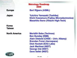
International Technology Roadmap for Semiconductors Metrology Roadmap 2012. Metrology Technical Working Group. Metrology Roadmap 2012 Spring and Summer Attendance. Europe Carlos Beitia ( CEA LETI MINATEC ) Philippe Maillot (ST) Japan Masahiko Ikeno (Hitachi High-Tech)

E N D
International Technology Roadmap for SemiconductorsMetrology Roadmap2012 Metrology Technical Working Group
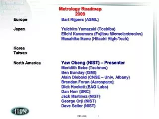
Metrology Roadmap 2012Spring and Summer Attendance Europe Carlos Beitia (CEA LETI MINATEC) Philippe Maillot (ST) Japan Masahiko Ikeno (Hitachi High-Tech) Yuichiro Yamazaki (Toshiba) Korea Taiwan North America Alain Diebold (CNSE) -Chair Christina Hacker (NIST) – co Chair David Seiler (NIST) Yaw Obeng (NIST) Benjamin Bunday (SEMATECH) Karey Holland (FEI) Scott List (Intel)
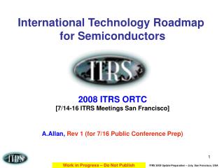
200K 20K 2K Metrology/Char. Research Tool Metrology Beta Tool w/precision Metrology Product Tool w/prec. & Uncert. Metrology Alpha Tool 200 20 First Tech. Conf. Device Papers Up to ~12yrs Prior to Product 2 0 24 -96 -72 -24 -48 Metrology Timing Model w/Technology Cycle Timing Production Research Development Process Research Tool Alpha Tool Beta Tool Product Tool Volume (Wafers/Month) 1st 2 Co s Reach Product First Tech. Conf. Circuits Papers Up to ~ 5yrs Prior to Product Months 2011 2013 2015 2017 2019 2021 Source: 2009 ITRS - Executive Summary Fig 2b
Metrology for Lithography CD-SAXS Contour vs Design Critical Dimensional Metrology is extended beyond Traditional Line Edge Roughness CD Metrology Extendibility Potential Solutions Multiple Patterning 2p CD p/2 Block co-polymers Scatterometry - Mueller Matrix Ellipsometry Spacers Litho Metrology for 3D Transistors Peter Clark ee Times 5-17-12
Area of Great Industry Interest Mask Metrology for EUV Lithography Mask Substrate Defect Inspection Mask Blank Inspection Absorber Layer Absorber Layer Absorber Layer Mo-Si Multi Layer Glass Glass Glass Glass 2 defect types: phase and amplitude defects Patterned Mask Inspection Actinic AIMS Aerial imaging measurement system Project what mask will print onto a CCD detector
Complex structures such as FinFETs require 3D metrology Many parameter (see diagram), not counting top corner rounding, footing, or etch recess under fin. Gate spacer would increase number of parameters. One example from 2011 SPIE: Fin is measured by CD-SEM or AFM and results fed forward OCD (scatterometry) then simultaneously measures fewer parameters with improved measurement uncertainty and higher speed. All methods are advancing : Complementary metrology delivers better solution Challenge: Dimensional metrology on complex 3D structures requires many parameters to be measured simultaneously 3D Transistor Dimensional Metrology gate 1 parameter 3 parameters HM 3 parameters fin HiK/MG 3 parameters 2 parameters Intel, May 2011 gates fins Require measurements of fin CD, height, sidewall angle and roughness.
CD-SEM Extendability Better CD SEM Via better image acquisition Traditional frame averaging Drift-corrected frame averaging Fast single frame 3D model determines all structure dimensions AndrasVladar, NIST
Metrology for 3D Transistors and Memory + III/V and Ge High µAlternative Channel Mat’ls EOT & Defects for New Channel Materials for high µ Metrology for Next Generation Metal Gate/High k stacks 3D Metrology for Advanced Memory Nano-topography & Local Stress measurements CD/Sidewall/Height/Stress/Dopant Metrology for 3D Devices MuGFET MuCFET FDSOI New Memory Materials Phase Change Memory
Metrology for New FEP Memory • Resolving Redox Memory • What is the switching mechanism(s)? • How does it form? Can we see filaments? • Is it reversible? Proposed mechanism: Reversible Metal Filament Proposed mechanism: Mobile Oxygen Vacancies Tong, et al, IEEE Transactions on Nuclear Science, 57,(2010), p 1640 Sakamoto et al., APL 91 092110 (2007)
Properties of next Gen High k stacks New Materials impact CD Metrology • Resolving New Materials and Processes • What is the crystal structure? • What is the correlation between electrical properties & materials structure? • How can interfaces be engineered? XRD SE GI-I- XRD & Texture Theoretically determined k values X. Zhao and D. Vanderbilt, Phys. Rev. B., 233106 (2002) Hill et. Al. J. Appl. Phys. 103, 093712 2008 higher-k high-k wavelength XAS
Metrology for 3D Interconnect New subchapter for 3D Interconnects introduced in 2011 Overlay Through Silicon Substrate – IR Microscopy TSV Metrology and Inspection: X-Ray Microscopy Stress Metrology around TSVs Raman Microscopy Bonding Defects – SAM Scanning Acoustic Microscopy Voids and Delamination
High carrier mobility and structural robustness have driven a considerable effort in Graphene research Metrology for ERM / ERD Defects in CVD Graphene Quantum Hall Effect observes the Berry Phase Newly Recognized Gaps • Measurement of Contact Resistance for Nanostructures • ESH measurement requirements for new materials and nanomaterials • Metrology to identify sub-10ppm metallic CNTs in semiconducting CNTs • High Throughput Characterization of 3-D Defects in DSA films • Effective measurements of polymer segregation on surfaces for DSA use • Non-destructive characterization of local buried interface properties and structure. E.g., buried graphene on dielectrics, topological insulators, deterministic fabrication.
Modeling, Simulation, and Metrology • Need to connect multiple measurements/methods at nanoscale to properties in a large area using modeling and simulation • Example : Simulations of SRAM cell show that each transistor experiences a different stress field – measuring one transistor does not represent the entire SRAM Cell I - V Final Stress in SRAM Cell “Sentaurus TCAD simulations from Synopsys – TCAD News Dec 2010”
Metrology Summary 3D Metrology • Litho • Litho Metrology Now 3D • Fin, Double Patterning Requirements • FEP • USJ Metrology Gap (profile and dose) • Defects in new channel materials Ge and III-V ‘s • Interconnect • Void Characterization now R&D • K values of patterned films • ERD-ERM • Contact Resistance Measurement Gap • ES&H • Many Measurement GAPS From Dick James – Chip Works SST Blog CVD Graphene F. Nelson CNSE