Download
1 / 26
260 likes | 434 Vues
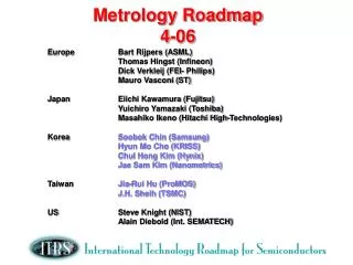
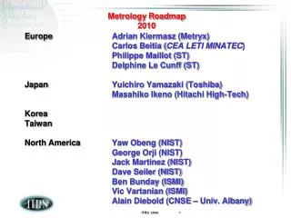
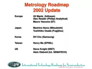
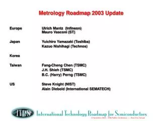
Metrology Roadmap 2003 Update. Europe Ulrich Mantz (Infineon) Mauro Vasconi (ST) Japan Yuichiro Yamazaki (Toshiba) Kazuo Nishihagi (Technos) Korea Taiwan Fang-Cheng Chen (TSMC) J.H. Shieh (TSMC) B.C. (Harry) Perng (TSMC) US Steve Knight (NIST)

E N D
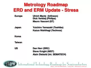
Metrology Roadmap 2003 Update Europe Ulrich Mantz (Infineon) Mauro Vasconi (ST) Japan Yuichiro Yamazaki (Toshiba) Kazuo Nishihagi (Technos) Korea Taiwan Fang-Cheng Chen (TSMC) J.H. Shieh (TSMC) B.C. (Harry) Perng (TSMC) US Steve Knight (NIST) Alain Diebold (International SEMATECH)
AGENDA • 2003 ITRS Changes • Lithography Metrology • FEP Metrology • Interconnect Metrology • Integrated Metrology and APC • Key Challenges
Metrology Critical Challenges Five Difficult Challenges ³ 45 nm, Through 2009 • Metrology Integration and APC • Starting Materials and In-line Metrology for strained Si, SiGe, and SOI • Control of high-aspect ratio technologies including copper void detection • Measurement of complex material stacks and interfacial properties • Measurement test structures and reference materials
Metrology Critical Challenges Five Difficult Challenges < 45 nm, Beyond 2009 • Nondestructive, production worthy, wafer and mask level microscopy for CD and overlay • New strategy for in-die metrology must reflect across chip and across wafer variation • Statistical limits of sub-45 nm process control • Structural and elemental analysis at device dimensions. i.e. materials characterization • Development of manufacturing metrology when device and interconnect technology remain undefined
Practical vs Desired Implementation of P/T • Evaluation of CD measurement capability done using sample with single shape and CD • This misses changes in accuracy and precision due to line edge roughness and sidewall angle, etc. • Propose : Total Measurement Uncertainty (TMU) Defines a new precision (P in the P/T ratio) P(TMU). P(TMU) should be determined on technology representative set of samples that accounts for variations in measurement bias associated with each process level.
16 nm Node - 2018 6.35mm Importance of Mask CD Tables CD Control Starts at the Mask Overlay and CD Control after Exposure 152mm 152mm 40 nm mask line width 20 nm scattering bars CD Control after Etch 10 nm printed line width EUV 7 nm physical line width Litho Metrology
Litho Process part of total CD budgetRevised 9-03 • Litho Process range Feature Process Range 3Litho/Etch Division • Isolated Gate10%Litho 4/5 Etch 1/5 • Dense Lines 15% Litho 2/3 Etch 1/3 • Contacts 10% Litho 2/3 Etch 1/3 • Use Process Range for Physical (Etched) Gate for both Printed and Etched Gate • Variances add as sum of squares • Make Precision of Printed gate match that of Etched Gate and Result is that Printed Gate now requires better precision
Litho Process part of total CD budget • LER becomes LWR and LWR= 8% of CD • Assume LWR= 2 * LER • Statistical Models used by Litho TWG to divide this variation between • Lens Aberration • Reticle CD variation • Inaccurate optical proximity corrections • Illumination effects
Binary Mask Alt. Phase Shift Mask s1 = mask CD variation R1 = Mask Error factor R2 = Lens Error R3 = Bake Temp DCD/DT DT R4 = Focus and Dose Variation 90 nm node 65 nm iso lines Sergei Postnikov and Scott Hector: Motorola for Litho TWG Dose and focus control errors are largest component of litho CD process range
single value from distribution average Distribution of linewidths inside test structure test structure inside a die What are you Measuring?
Commercially available R&D Software comparison of top down line scan of edge to golden image Tilt Beam SEM Scatterometry CD-AFM Dual Beam FIB (destructive) Software to convert top down image to 3D image All suppliers appear to offer tilt beam now 3D CD Metrology SEM – Scatterometry – CD-AFM
FEP : High Metrology • Metal Gate and high k both require metrology development • SOI and Strained Silicon already in initial testing • New Transistor Designs being Developed
New Device Designs impact Metrology How do we measure gate dielectric thickness on sidewalls?
Metal Gate impacts selection of Metrology q Models can include interface layer d Phase shift = q 2 d sin l • If Metal Gate is used then either • Integrate metrology with process tool • try X-ray Reflectivity Thanks to Rich Matyi 4 nm HfO2
Gaps in Interconnect Metrology • VOID Detection in Copper vias & lines now based on 1/10 via diameter • Barrier/Seed quality on sidewalls • Killer Pore Detection in Low kpore size distribution • Non destructive metrology for adhesion and (at operating freq.) for patterned wafers
5 nm layer of Ge on top of 4 nm SiOx 10 nm p-Si core diameter & 10 nm i- Ge layer 500 nm L.J. LAUHON, M.S. GUDIKSEN, D. WANG & CHARLES M. LIEBER Nature 420, 57 - 61 (2002) Nanowire Transistors and Interconnect
SENSOR based Integrated MetrologyComments on: Advanced Process Control - Advanced Equipment Control Components of Solution • APC, including Run-to-run control • FDC: Fault Detection and Classification • Integrated Metrology
APC and Integrated Metrology • APC GOAL : model based predictive control based on process and metrology models using in-situ and in-line measurements • APC is prevalent for CMP, Lithography (Overlay and CD) and Etch, in many cases required • Scrap prevention through Fault Detection and Classification is driving sensors/metrology • Integrated Metrology is viewed as critical to support APC
Key Metrology Challenges • Breakthrough microscopy for CD measurement • Measurement capability for control of interface between high and substrate & gate electrode • Low killer pore detection and copper void control • Atom by Atom microscopy for materials characterization
Line Edge Roughness Replace LER with LWR. It will be assumed that LER requirements, if they arise independently of linewidth considerations, will be given by . It was proposed that the LWR numbers in the roadmap should be 8% of the final linewidth. Lower frequency range of LWR is designed to distinguish between CD changes and linewidth changes
Line Edge Roughness LWR will be 3s of the linewidth over a range of spatial frequencies given by P is the pitch and is the low-end-of-range of the drain extension The upper end of the spatial frequency range derives from considerations of diffusion. Dopant will diffuse under the roughness that varies much faster than dopants will diffuse under the rough parts of the gate.
100M 200K Development Production 10M 20K 1M 2K Volume (Parts/Month) Alpha Tool Beta Tool Production Tool 100K Volume (Wafers/Month) 200 10K First Two Companies Reaching Production 20 First Conf. Papers 1K 2 0 12 24 -24 -12 Months Source: 2001 ITRS - Exec. Summary Figure 2 3 Work in Progress – Do Not Publish Original 2001 ITRS (Unchanged in 2002 Update) Production Ramp-up Model and Technology Node “Figure 2”