Advanced Test Structures for Semiconductor Analysis
Explore key measurements like Diode C-V, strip capacitances, and MOS structures to understand semiconductor behavior. Results from HPK-L1 test structures offer insights into depletion voltages, coupling capacitors, and more. Dive into detailed comparisons and interpretations from Bernhard and Lehner at U. Zurich. Gain valuable insights into material properties, processing techniques, and resistance values for accurate semiconductor testing.

Advanced Test Structures for Semiconductor Analysis
E N D
Presentation Transcript
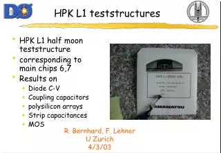
HPK L1 teststructures • HPK L1 half moon teststructure • corresponding to main chips 6,7 • Results on • Diode C-V • Coupling capacitors • polysilicon arrays • Strip capacitances • MOS R. Bernhard, F. Lehner U Zurich 4/3/03
HPK L1 teststructures • depletion voltage of diode ~110V • Corresponding sensor (HPK-L1 #6,7) depletion voltages: • 150V (HPK) • 130V (KSU), 110V (FNAL) • N.B. depletion voltage of segmented strip detector is ~5-10% higher than planar diode
HPK L1 teststructures • coupling capacitor test structure • same length than on sensor: 7.74 cm • low frequency limit: 115 pF => 14.8 pF/cm (in specs)
HPK L1 teststructures • CC breakdown ~220-230 V • similar to HPK-L2
HPK L1 teststructures • Aluminum trace teststructure (meander-like) • length 60 mm • resistance: 35 Ohm/cm (spec: 30 Ohm/cm) • HPK-L2: 16 Ohm/cm, smaller due to wider Al traces
HPK L1 teststructures • p+ implant structure • 130 kOhm/cm (on HPK-L2: 104 kOhm/cm)
HPK L1 teststructures • numerous polyresistor structures • different arrays: PS0, PS10, PS20, PS30 and PSH0 – PSH30 • What is the difference? • polysilicon material? • Processing? • doping?
HPK L1 teststructures • linearity from in range from –5V to +5V given for PS-30 and PS-20 resistor array • PS-10 and PS-0 have breakdown at ±2V • in linear region all resistors measured to be 1.05 ± 0.01 Mohm
HPK L1 teststructures • Baby detector w/ polysilicon resistors • R_poly: 0.7 ± 10% Mohm • R_poly + R_implant: • 1.5 ± 10% Mohm • implant alone: 130kOhm/cm • 1MOhm implant for 7.7 cm strip • not fully consistent !
HPK L1 teststructure • exact resistance value is difficult to measure, currents are low • value is irrelevant though, as long as R_inter >> R_poly • R_inter on babydetector ~ 10 Gohm (?)
HPK L1 teststructures • total strip capacitance • includes both neighbors • plus backplane capacitance • capacitance reaches plateau at ~10V • frequency dependence: Capacitance at 1 MHz: ~8.5pF Cap/cm: ~1.1 pF/cm
HPK L1 teststructures • interstrip capacitance • to one neighbor: ~3 pF => 0.39 pF/cm • to both neighbors: ~5.5 pF => 0.71 pF/cm
MOS structure • MOS (metal-oxide- silicon) structure • measure flatband voltage • use only 0.1V oscillator amplitude on LCR • high frequency (200kHz) • flatband shift to negative values? • interpretation not yet clear