Download
1 / 19
190 likes | 215 Vues
This overview provides information on the CMS HPK campaign, which focuses on the development and testing of planar silicon sensors. The campaign includes a survey of available silicon materials, the investigation of different sensor layouts, and the measurement of various electrical parameters. The overview also discusses the use of device simulations and ongoing research on potential additional sensor candidates. Additionally, it covers the production and characterization of different sensor structures, including diodes, mini sensors, and pixel sensors. The irradiation of sensors and the study of damage caused by different particles are also discussed.

E N D
The CMS HPK campaign - An overview Alexander Dierlamm
CMS Strategy • Most of the volume of a future Tracker will be equipped with planar silicon sensors • We have started a survey of available silicon materials to probe their individual limits • One wafer layout has been developed and the various materials are processed with this mask by the same producer, which allows well defined comparisons • We investigate the properties of several layout options for strip, strixel and pixel sensors • A well defined measurement plan has been worked out and participating institutes have been inter-calibrated to guarantee comparable measurements • For the test wafers a producer was chosen, that can provide the large quantity and high quality we need “HPK campaign” • Measurements are complemented by device simulations • In parallel, there are R&D projects on potential additional candidates for the most inner layer(s) • 3D silicon sensors (production with Sintef, FBK, CNM) • Diamond sensors 18th RD50 Workshop
200µm low conc. 120µm high conc. HPK campaign – Materials • Initially ordered production of 126 wafers delivered completely • Part of thin FZ wafers came “deep diffused” showing some features, which makes a comparison with physical MCz difficult • “Deep diffused” wafers are about 20% cheaper than 200µm thin wafers! We will investigate this option… • Additional material ordered lately and expected Sept./Nov. 320µm FZ200 deep diff. 18th RD50 Workshop
320µm 200µm 120µm 120µm 200µm 320µm Investigation of “deep diffused” material • Unusual behaviour of thin “deep diffused” material • Well seen in IV and CV of diodes • Thin diodes show non-abrupt depletion behaviour • Volume generated currents are higher than in thick diodes • But currents are still very low (<1.5µA/cm³ @ 500V)! 18th RD50 Workshop
HPK wafer layout 18th RD50 Workshop
Structures and goals • Diodes • Material characterization and add. annealing studies • Measure IV, CV, CCE, TCT, DLTS, TSC, photo cond., … • Mini sensor I (Baby_std) • Material characterization, charge collection • Measure IV, CV, strip para., CCE, e-TCT • Mini sensor II (Add_Baby) • Material characterization using different radiation sources • Measure IV, CV, Lorentz angle • Sensor with integrated PA (Baby_PA) • Layout study: spare glass PA • Measure strip capacitances, CC, signal coupling • Sensor with short strips and edge read-out (Baby_strixel) • Layout study: read-out lines from inner strip to outer edge • Measure strip capacitances, CC, signal coupling • Test structure field (TS) • Process qualification • Measure many things incl. SIMS, SRP, SEM, … • Pixel • Real size pixel sensor for CMS ROC footprint • Measure IV, efficiency, σ • Multi-geometry strip (30mm) sensor (MSSD) • Layout study: strip width and pitch variations • Measure CV, IV, Cint, S/N, σ • Multi-geometry pixel (1.25mm/2.5mm) sensor (MPix) • Layout study: pixel length and pitch variations • Measure CV, IV, Cint, Rpoly/RPT, S/N, σ Diode Baby_std Baby_PA Baby_strixel Pixel 18th RD50 Workshop
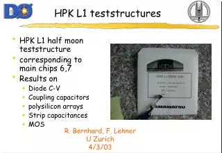
Baby_std • A “standard” mini strip sensor with 256 strips and 80µm pitch • Evaluation of all electrical parameters • Measurement of charge collection with beta-source and LHC-like read-out system • Edge-TCT can provide E-field and charge collection vs. thickness profile on sub-set 35.12mm 22.62mm ALiBaVa setup at KIT 18th RD50 Workshop
Multi-SSD • Contains 12 regions with different strip sensor layouts • This is a replica of the famous test-structure, which brought us the conclusion that the total strip capacitance is a function of w/p only (demonstrated for 0.2<p/d<0.8 and 0.1<w/p<0.6) [CMS Note 2000/011] • This time we check thinner material (0.2<p/d<2.0) and higher irradiation! 32.80mm 65.74mm 18th RD50 Workshop
Multi-Pixel 22.45mm • Contains 12 regions with different pixel/strixel layouts • Pixel size in the regime of pixellated pT layers • Study inter-pixel capacitances and different biasing schemes • Special PA to read-out with APV25 in beam test 54.66mm 18th RD50 Workshop
Irradiation fluences • Need to understand damage by neutron, charged hadron and mixed particle irradiation • Fluences chosen for conditions at various radii • Neutron fluence slightly adapted to get info on increasing neutron fluence • Annealing steps chosen to cover initial short term and long term annealing: * 156min at 60°C ~ 15min at 80°C 18th RD50 Workshop
Irradiation sequence • Initial measurements of all parts • Irradiation with n/p • Short annealing 10min @ 60°C • Measurement of devices • Irradiation with p/n • Short annealing 10min @ 60°C • Measurement of devices for several annealing steps TRIGA reactor, Ljuljana Proton cyclotron, KIT n-Irradiation n-Irradiation p-Irradiation Mixed particle damage Single particle damage p-Irradiation 18th RD50 Workshop
Firenze Bari 17 institutes currently involved in HPK campaign Size of logos has no meaning!!! 18th RD50 Workshop
Latest activities • Initial qualification of structures and materials ongoing • Most participating institutes perform measurements routinely • Measurement results are being uploaded to a dedicated database (essential for more than 5000 pieces!) • Deep diffusion material investigated on diodes before and after irradiation (protons and neutrons each 1e14neq/cm²) • Next talks by Joachim Erfle (UHH) and Robert Eber (KIT) • Talk from Alexandra Junkes (UHH) yesterday • Complete mixed irradiation scenario exercised on FZ part of Add_Baby, which will be used for dedicated Lorentz angle studies • Talk by Andreas Nürnberg (KIT) at 15:00 • First beam test with MSSD and MPix structures successfully performed at FNAL • Talk by Panja Luukka (HIP) at 14:40 • Special strixel read-out and PA on sensor being investigated (coupling of routing lines and PA layouts will also be studied on 2. metal wafers) 18th RD50 Workshop
BACKUP 18th RD50 Workshop
Baby_PA • Signal almost homogeneous when charge is generated (by Sr90 source) on normal region • Strong signal drop (~30%) when charge is generated in PA region (~2.5mm), where signal is lost to other channels due to the crossing read-out metallization 18th RD50 Workshop
Baby_PA 18th RD50 Workshop
Baby_PA 18th RD50 Workshop
strip 177 strip 175 strip 190 strip 192 strip 191 Baby_strixel • Scan with IR laser between two strips • Scan in far region shows no induced charge on near implantation • Scan in near region shows a strong induced charge on read-out metal running between near implantation • Signal is high enough to mimic charge generation in far region more advanced cluster algorithm needed! 18th RD50 Workshop
MSSD testing • IV, CV and Cint on all 12 regions of sensor automatized by switching matrix and ready for cold measurements in insulated box • Additional beta setups are being setup to measure S/N and charge sharing • Available at Florence and CERN; FNAL setting up 18th RD50 Workshop