Power Distribution Studies at Fermilab
170 likes | 291 Vues
This document outlines the power distribution studies conducted at Fermilab, focusing on the panel test stand, system setup, and DC-DC conversion tests. Key topics include efficiency measurements, the impact of cooling on converters, and pixel performance evaluations. The studies utilized AMIS2 DC-DC converters and involved thorough measurements of analog signals, temperature impacts, and noise levels. Summarized conclusions highlight ongoing power integrity tests and future measurements for enhanced understanding of powering schemes and efficiencies.

Power Distribution Studies at Fermilab
E N D
Presentation Transcript
Power Distribution Studies at Fermilab Aida Todri, FNAL ATLAS/CMS Power WG Meeting March 31st , 2010
Outline • Panel test stand. • System setup. • DC-DC conversion powering scheme tests: • Efficiency measurements. • Cooling impact on converter. • Pixel performance measurements.
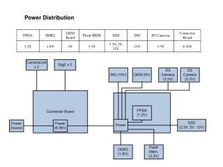
Panel Test Stand • CAPTAN • DAQ system, 12bit ADC, 65MHz • Panel • 21 ROCs, TBM, 40MHz, Ianalog~1.35A, Idigital~1.5A with external load • Converters • AMIS2 DC-DC converters for VA and VD.
Pixel Calibration Analog signal in ADC counts from all the readout chips in a panel sampled by the front-end digitizer. Decoding of analog signal.
DC-DC Converters • Chip: AMIS2 by CERN • Vin=6-12V • Iout<3A • Vout=3.3V • fs=600kHz..3MHz • PCB: Aachen • 2 copper layers • External air-core inductor • L=550nH, R=80mΩ AMIS2
Impact of Chip Cooling • Observation : Cooling the converter chip ~20˚C impacts the regulator and decreases the voltage level being supplied to the panel. • Cause degradation in the signal pulse. no cooling w/ cooling
Temperature Measurement no cooling with air fan cooling Ton_chip=70˚C Ton_chip=69˚C Ton_ind=106.8˚C Ton_ind=88˚C
Power Supply Noise No converter w/ DC-DC converters ∆=278mV Vout=2.42V Vout=3.26V, Vin=9V Temp=62.8˚C
Performance Measurements S-Curve Test: • To measure the signal threshold and noise level of each pixel. • Efficiency of the pixel is derived as a function of the amplitude of the calibration signal. • Each pixel response is obtained by injecting calibration pulses with different Vcal DAC values (1Vcal=65e). • S-Curve calibration is run with and without DC-DC converters.
Serial Powering Test Stand • SPi Chip: FNAL • Vshunt=1.2 to 3V • Iseries=0 to 4A • CAPTAN sending data packets to program the SPi chip to operate at different modes. • SPi powered through a power supply source by limiting current. • Limited current output to drive a plaquette or panel • Used ~ 250mA
CAEN A4603 DC-DC Conversion Panel Next Test Setup • Setup modified CAEN A4603 module to power up the chips • Perform test a lower temperatures (chiller box) • Perform test with a magnet 1.5T.
Conclusions • Currently: • Performing power integrity tests on the panel system • Performing pixel performance measurements • Characterizing the DC-DC converter and serial powering schemes and their efficiencies • Next Steps: • Continue with performance measurement studies for DC-DC powering scheme. • Complete test stand setup using: • CAEN power supply, magnet, cooler temps. • Testing of serial powering scheme • Efficiency comparisons between two schemes.