Transition Converter
This document outlines the design and implementation of a Transition Converter that facilitates the processing of signals from new antennas for compatibility with existing correlator systems at the VLA. It describes the architecture, which includes digital FIR filters that handle 1 GHz bandwidth data from 8-bit digitizers to produce 50 MHz outputs. The implementation strategy involves using Xilinx Vertex II FPGAs, focusing on optimizing hardware resources and power dissipation. The transition converter aims to ensure seamless signal transition with necessary spares and efficient usage of hardware.

Transition Converter
E N D
Presentation Transcript
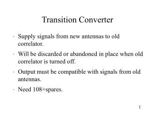
Transition Converter • Supply signals from new antennas to old correlator. • Will be discarded or abandoned in place when old correlator is turned off. • Output must be compatible with signals from old antennas. • Need 108+spares. 1
Transition Converter • Processes 1GHz bandwidth data from 8 bit digitizers. • Uses digital FIR to produce 50MHz bandwidth data. • D/A converter produces analog signal input to VLA T4 filter modules. 2
Digital Filter • Input is 8:1 demultiplexed data from DTS. • 2 stage linear phase FIR architecture. • First stage is an anti-alias bandpass 8:1 decimator. • Second stage is a half band 2:1 decimator. • Spectral inversions used to arrange to put second stage cutoff at VLA DC. 3
First stage • Selects 1 of 8 sub bands created by 8:1 demultiplex of DTS data. Nominally sub band 5. • Uses polyphase architecture to process 1GHz bandwidth at 256MHz clock rate. • Sampling theorem is not violated, bandpass cannot be greater than 1 sub band width. • Provides anti alias processing for second stage. 4
Second Stage • Controls DC band edge at VLA T4 input. • Cutoff must be sharp to prevent aliasing of image frequencies into VLA input. • Uses half band architecture to exploit symmetries of filter coefficients to reduce required hardware by nearly ½. • 2:1 decimation produces output clock rate of 128MHz. 5
Spectral Inversion • Works like mixing against a sine wave sampled at positive and negative peaks. Normalized frequency of 0.25. • Multiply every other sample by -1. • Symmetry of DFT suppresses images. • Works. 6
Half Band FIR • Linear phase filter has symmetric impulse response. • Half band odd length FIR has every other impulse response output identically equal to zero except center sample. • Other half of responses have cosine symmetry. • Symmetries greatly reduce required hardware for implementation (nearly 1/2). 7
Hardware Implementaion • Implemented in Xilinx Vertex II series FPGA. • Space permitting will be implemented in FPGA on DTS fiber receiver board. Otherwise on temporary host boards, this would complicate operations when both correlators are in use. • Using Carlson's formulas for estimating resources approximately 4800 Virtex II logic slices. 10
Hardware Implementation • Stage 1 - 100 Tap 8 bit data 8 bit quantized filter coefficients = 2571 slices. • Stage 2 - 511 Tap half band 4 bit data 10 bit quantized coefficients = (exploiting symmetries) 2228 slices. • 5000 slices + auxilliary functions. • Treat these size estimates the way an astronomer would distance estimates. • VLA correlator ~10,000-20,000 slices equiv. 11
Hardware Implementation • XC2V1000 - 5,120 slices $400. • XC2V1500 - 7,680 slices $700. • XC2V2000 - 10,752 slices $950. • Source Avnet web site fall 2001. • If implemented on DTS receiver room for receiver functions is also needed, shares costs with permanent hardware. XC2V1500 looks adequate. • $200 change per unit = >$20,000 total change. 12
Power Dissipation • Wide band noise inputs tend to maximize power dissipation. • Excess power dissipation shortens life of FPGA. • Total power, in absolute terms, is not great but it is being dissipated in a small volume. • Will effect packaging. 13