Download
1 / 1
10 likes | 165 Vues
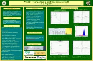
ACSES – your partner in analyzing the nanoworld. D. S. Karpuzov. ACSES, CME-607, University of Alberta, Edmonton, AB, T6G 2G6. Samples of our recent data. Instruments. What is ACSES. High-resolution spectra. Low-resolution spectra.

E N D
ACSES – your partner in analyzing the nanoworld D. S. Karpuzov ACSES, CME-607, University of Alberta, Edmonton, AB, T6G 2G6 Samples of our recent data Instruments What is ACSES High-resolution spectra Low-resolutionspectra • XPS Spectrometer AXIS 165 (Kratos) equipped with ISS, AES, SEM (operational) • XPS Imaging Spectrometer ULTRA (Kratos) with TPD and ISS (operational) • ToF SIMS iV (TOFSIMS) (operational) • Multifunctional System including • MBE and EBE (Createc, installed) • EELS and LEED (SPECS, installed) • JAMP 9500F Auger Microprobe (Jeol, tested, due in September 2004) • FTIR Spectrometer with controlled environment (in Fall 2004) • STM/AFM microscope with environment control (in late 2004) ACSES is the acronym for Alberta Centre for Surface Engineering and Science, an interdepartmental facility created jointly by the Faculty of Science and Faculty of Engineering at the University of Alberta ACSES Mission To provide comprehensive surface characterization of materials for academics as well as R&D and industrial work in Western Canada Modification of C1s peak of poly-styrene and poly-methyl-methacrylate after treatment in plasma Broad spectrum of NiCo thin layer on Si Techniques • ACSES is committed to run the following techniques: • Surface analysis: • XPS (X-ray Photoelectron spectroscopy) • XPS imaging • AES (Auger Electron Spectroscopy) • SAM (Scanning Auger Microscopy) • Static SIMS (Secondary Ion Mass Spectroscopy) • ISS (Ion Scattering Spectroscopy) • EELS (Electron Energy Loss Spectroscopy) • LEED (Low Energy Electron Diffraction) • SEM (Scanning Electron Microscopy) • TPD (Temperature Programmed Desorption) • Surface FTIR (Fourrier Transform Infrared Spectroscopy) • STM/AFM (Scanning Tunneling Microscopy/Atomic Force Microscopy) • Surface Treatment / Deposition: • High-temperature/pressure catalytic reactions • MBE (Molecular Beam Epitaxy) • EBE (Electron Beam Evaporation) How to reach us? For contact information and details about the instruments please visit our website www.ualberta.ca/ACSES Left – concentration report derived from the NiCo spectrum above, Right – lateral distribution of Ni for the same sample C-H (in blue), C-O (red), and C=O(pink) components in C1s spectrum of PET Our Sponsors Angular resolved XPS. From the well resolved peaks of Si-Si and Si-O the oxide thickness can be evaluated Depth profile of composition, MnO2/Pt/Si. 3 keV Ar beam, 45 degr. incidence. Etch rate 0.4 nm/min