Progress on the Silicon Drift Tracker R&D program
Progress on the Silicon Drift Tracker R&D program. Rene Bellwied (Wayne State University) for the SDT group WSU (R. Bellwied, D. Cinabro, V. Rykov, Y. Guo) BNL Physics ( F. Lanni, D. Lissauer, V. Jain) BNL Instrumentation (W. Chen, Z. Li, V. Radeka)

Progress on the Silicon Drift Tracker R&D program
E N D
Presentation Transcript
Progress on the Silicon Drift Tracker R&D program Rene Bellwied (Wayne State University) for the SDT group WSU (R. Bellwied, D. Cinabro, V. Rykov, Y. Guo) BNL Physics ( F. Lanni, D. Lissauer, V. Jain) BNL Instrumentation (W. Chen, Z. Li, V. Radeka) Linear Collider Workshop, UT Arlington, Jan. 9-11, 2003 Proposed layout for LC tracker Silicon Drift technology benchmarks Hardware R&D plans Software update Summary and Outlook
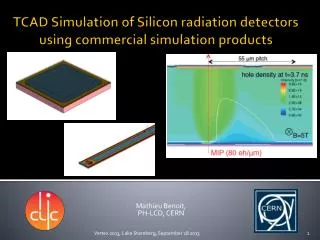
Silicon detector option for LCD(small detector, high field B=5T) Central tracker: Five Layer Device based on Silicon Drift DetectorsRadiation length / layer = 0.5 %, sigma_rphi = 7 mm, sigma_rz = 10 mm Layer Radii Half-lengths ----------- ------------ 20.00 cm 26.67 cm 46.25 cm 61.67 cm 72.50 cm 96.67 cm 98.75 cm 131.67 cm 125.00 cm 166.67 cm 56 m2 Silicon, Wafer size: 10 by 10 cm, # of Wafers: 6000 (incl. spares) # of Channels: 4,404,480 channels
R.Bellwied, June 30, 2002 SDD’s: 3-d measuring devices Features: Low anode capacitance = low noise 3d information with 1d readout Pixel-like by storing 2nd dimension in SCA Low number of RDO channels based on charge sharing
Typical SDD Resolution • Can be improved through: • faster drift, • stiffer resistor chain for voltage gradient, • different anode pitch, • and better starting material
STAR-SVT characteristics • 216 wafers (bi-directional drift) = 432 hybrids • 3 barrels, r = 5, 10, 15 cm, 103,680 channels, 13,271,040 pixels • Pixel count determined by # of ‘time buckets’ in Switched Capacitor Array • Resolution: 8 micron and 17 micron respectively, two-track: 150 micron • Very high resistivity NTD n-type Silicon with no driving capability. At least preamplification stage has to be on detector • Radiation length: 1.4% per layer • 0.3% silicon, 0.5% FEE (Front End Electronics), • 0.6% cooling and support. Beryllium support structure. • FEE placed beside wafers. Water cooling. • Future: 5 barrels, 6000 wafers, 4,400,000 channels, 0.5% rad.length per layer resolution: 7 micron and 10 micron respectively.
Present: 6 by 6 cm active area = max. 3 cm drift, 3 mm (inactive) guard area Max. HV=1500 V, max. drift time=5 ms anode pitch = 250 mm, cathode pitch = 150 mm Future: 10 by 10 cm active area Max. HV=2000 V Anode pitch, cathode pitch have to be optimized to give better position resolution (more channels = more money) Stiffer resistor chain dissipates slightly more heat on detector, but requires no off detector HV support and allows a more linear drift in drift direction (better position resolution) Proposed wafer R&D
R.Bellwied, June 30, 2002 Details of mask design Future: stiffer implanted resistors, no outside power supplies
Present: bipolar PASA & CMOS-SCA ( 16 channel per die, 15 die for 240 channels on beryllia substrate ) Multiplexing on detector, 8-bit ADC off detector (3m) Future: 0.25 micron (DSM) radiation hard CMOS technology for all three stages in one single chip (PASA, SCA, 10-bit ADC) Example: ALICE-PASCAL Proposed Frontend (FEE) R&D
Present: Be angled brackets with Beryllia hybrids mounted Future: carbon fiber staves with TAB electronics wrap-arounds Proposed mechanical R&D
Improve position resolution to 5mm Decrease or increase anode pitch from 250 to 100mm or 400 mm ? Stiffen resistor chain and drift faster. Improve radiation length Reduce wafer thickness from 300mm to 150mm Move FEE to edges or change from hybrid to SVX Air cooling vs. water cooling Use 6in instead of 4in Silicon wafers to reduce #channels. More extensive radiation damage studies. Detectors/FEE can withstand around 100 krad (g,n) PASA is BIPOLAR (intrinsically rad. hard.) SCA can be produced in rad. hard process. R&D for new wafer layout
Hardware deliverables in present 3 year proposal • 2003 hardwaredeliverables: new drift detector wafer layout according to R&D goals. Feasibility study of BNL stripixel technology vs. drift detectors. • 2004 hardware deliverables: large batch of prototype detectors, test radiation damage in test beam and with sources. Beginning design of new frontend electronics • 2005 hardware deliverables: complete design for CMOS DSM type frontend with reduced power consumption and potentially integrated ADC, test TAB bonding of frontend to detector prototype, produce large frontend prototype batch. Extensive test beam requirements for completed detector/FEE combination by end of 2005.
Stripixels:something new from BNL Alternating Stripixel Detector (ASD) Interleaved Stripixel Detector (ISD) Pseudo-3d readout with speed and resolution comparable to double-side strip detector on single-sided technology (Zheng Li, BNL report, Nov.2000). Attractive for faster speed and easier to manufacture than double-sided strip
Use particle beams in the momentum range from 100 MeV/c to several GeV/c Measure single particle and two-track resolution Check noise and repetition rate for frontend Check settling time and power consumption for RDO power-off mode during bunches Need for test-beam in 2004/2005
Detectors:SD and LD geometries as of March 2001. • Resolutions:SD – r = 7 , z = 10 ; LD - r = 100 ,z = 1400 . • Input data: -events at , “panpy-tt-500-010301-*D-sim-**.sio” files. • Tracking: codes from the “hep.lcd.recon” package. • Analysis: Modified “TrackEfficiencyDriver” code (W. Walkowiak) from “Snowmass-2001” CD tutorial. • Acceptance: Barrel trackers (+VXD) with forward disk (Endcaps) hits removed (smeared to “a parsec” = 100 m away). • Framework: Local JAS analysis • Tasks addressed: momentum resolution, tracking efficiency (ideal), missing energy, ghost energy, track timing, comparative study with TPC. • News since last meeting: detailed GEANT geometry files for two alternate layouts of SDT provided, tracking efficiency and occupancy (with background) Simulation framework
STAR central Au-Auevent: inner layer: ~15 hits/hybrid (2% occupancy) 30,720 pixels per hybrid, 40 pixels/hit With same layout and LC simulations including g background according to T. Maruyama): Around 2000 g/event leave hit in Silicon, corresponding to an occupancy of 13 hits/hybrids (0.5% occupancy) 51,200 pixels per hybrid, 20 pixels/hit Occupancy could be further reduced by factor 2 by using different SCA Simulation update:hit occupancy on single wafer
For 100% hit efficiency: (97.3±0.10)% Almost identical to no background ! Occupancies and tracking efficiencies with background
Future SDT software R&D • 1.) optimize 3d tracking code for solid state tracker, compare performance to gas detector and other silicon technologies • 2.) write slow simulator for detector response • 3.) apply STAR tracking and pattern recognition for comparison • 4.) simulate two track resolution
What’s next for the SDT ? • Three year NSF proposal: 2003-2005 for a total of $450 K ($ 80, 170, 200 K) • Hardware contribution per year (for BNL): $ 25, 50, 90 K • The project has to grow, we need more groups interested in SDD (as of now only WSU and BNL expressed interest). • Prototype detectors for use in test setups at universities or other National Labs are available through WSU/BNL. • People with mask design skills could work on new prototype layouts. • The wafer and frontend electronics R&D could be split in two projects. • Readout electronics and DAQ integration have not been addressed at all. • Software development and simulations needs a lot more manpower. Talk to us if you’re interested (bellwied@physics.wayne.edu) • Check out the web at: http://rhic15.physics.wayne.edu/~bellwied/nlc