Download
1 / 50
630 likes | 1.51k Vues
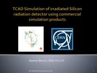
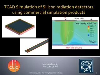
Mathieu Benoit, PH-LCD, CERN. TCAD Simulation of Silicon radiation detectors using commercial simulation products. Outline. Short summary of theory of Finite-Element / Difference Method (FEM) in Silicon TCAD simulation Numerical methods Existence of the solution Work Flow

E N D
Mathieu Benoit, PH-LCD, CERN TCAD Simulation of Siliconradiation detectors using commercial simulation products Vertex 2013, Lake Starnberg, September 18 2013
Outline • Short summary of theory of Finite-Element / DifferenceMethod (FEM) in Silicon TCAD simulation • Numericalmethods • Existence of the solution • Work Flow • Comparison of main commercial TCAD simulation software • Physics • Functionality (user friendliness) • Example of TCAD simulation • Space-Charge Sign Inversion (SCSI) • Double peak in invertedsensors • Charge multiplication • P-Spray Insulation • Magnetic Field effects • Charge-Sharing in pixel sensors • Conclusion Warning this talk mightcontainsbavariansphericalcows Vertex 2013, Lake Starnberg, September 18 2013
TCAD simulation principles Discretization of the Domain Approximated solution to the equation to solve Aproximation of the solution spaceusing test function Vertex 2013, Lake Starnberg, September 18 2013
TCAD simulation principles : Beyond the standard model ! • It is possible for the main TCAD simulation to perform simulation athigherorders of Boltzmann Transport Equation : • The thermodynamic model • Continuityequationonly • Transport Time >> Energy Relaxation time • The hydrodynamic model • Energy balance takenintoaccount • Modelize Carrier Heating, Velocityovershoot Vertex 2013, Lake Starnberg, September 18 2013
TCAD simulation principles • The exact solution to the equationneeds to bedefinable as : • n canbeinfinite (or not, ex: simple diode etc) • In FEM, n isfixed by the number of degrees of Freedom (nDOF) • nDOFisfixed by the meshdefined in yourgeometry Vertex 2013, Lake Starnberg, September 18 2013
TCAD simulation workflow • Device Simulation Conditioning • ReduceComplexity (symmetry, dead area removal) • Remesh for Device simulation (reduceoxide/nitridemesh, increasebulk) • « Old-school » process simulation • Hard-coded pixel geometrywhendefiningprocessingsteps • Possibilityfor limitedparametrization • Process Flow simulation • Workwith GDSII files provided by your favorite vendor • Abstract description of the process • Device Simulation • Electric Field, RamoPotential • Capacitance • TransientBehavior • Thermal/Mechanical Stress Simulation • Simple description of the geometry and doping using an editor • Definegeometry (Shape,material) • Define doping profile (parametric description) • Post-Processing • Extract Profiles ( E(x,y,z) , etc) • Extract Values (Breakdown, DepletionPotential ) Vertex 2013, Lake Starnberg, September 18 2013
Process Flow Simulation • Process Flow simulation allowsfor more automatedstudies of differentgeometries • Generatemaskusingyour favorite software (pyGDS, Cadence, etc) • Use GDSII mask to definegeometry • Use abstract and parametric description of the process • Implantation, lithography, deposits, annealing etc… • TakesAdvantage of multiplication of available CPU/RAM in the HEP Community • Chose a set of geometrical/Process/Electricalparameter to scan • Launch simulation in parallelusing LSF Infrastructure Timepix 3x3 Pixel Mask set generatedusingpyGDS Structure Generatedusingprocess Flow Vertex 2013, Lake Starnberg, September 18 2013
Process Flow Simulation Vertex 2013, Lake Starnberg, September 18 2013
Importance of meshingproperly • Meshing in the first main problemyouwillencounterwhendoing TCAD simulation • Determination of the perfectmeshis not an exact science (a lot of trial and error ! ) • Upperlimit of mesh size set by devicefeature size (implants , electrodes) • Lowerlimit of mesh size set by computationallimits (RAM, computing time) • Meshingalgorithmavailable in software packages also have internal limitation (!!!) Vertex 2013, Lake Starnberg, September 18 2013
Physics (Device Simulation) Vertex 2013, Lake Starnberg, September 18 2013
Generation/Recombination • Modified Shockley-Read-Hall G/R • A sum of SRH contribution by each trap • Γ is the degeneracy of the trap, ni the intrinsic concentration of carriers Vertex 2013, Lake Starnberg, September 18 2013
Generation/Recombination electron emmision • Transient behaviour of traps σn,p is trap capture cross-section vn,pis thermal velocity ni is intrinsic concentration FtA,TD the probability of ionization NtA,TD space charge density electron capture hole capture hole emmision Electron capture Electron emmision Hole capture Hole emmision Vertex 2013, Lake Starnberg, September 18 2013
Radiation damage Non-ionizing Energy loss D. Menichelli, M. Bruzzi, Z. Li, and V. Eremin, “Modelling of observeddouble-junction effect,” Nucl. Instrum. Meth. A, vol. 426, pp. 135–139, Apr. 1999. F. Moscatelliet al., “An enhanced approach to numerical modeling of heavily irradiated silicon devices,”Nucl. Instrum. Meth. B, vol. 186, no. 1-4, pp. 171–175, Jan. 2002. F. Moscatelliet al., “Comprehensivedevice simulation modelingof heavily irradiated silicon detectors at cryogenic temperatures,” IEEE Trans. Nucl. Sci., vol. 51, no. 4, pp. 1759–1765, Aug. 2004. M. Petasecca, F. Moscatelli, D. Passeri, G. Pignatel, and C. Scarpello, “Numerical simulation of radiation damage effects in p-type silicon detectors,” Nucl. Instrum. Meth. A, vol. 563, no. 1, pp. 192–195, 2006. Ionizing Energy loss Vertex 2013, Lake Starnberg, September 18 2013
Impact ionization Selberherr, S.,"Analysis and Simulation of Semiconductor Devices", Springer-VerlagWien New York, ISBN 3-211-81800-6, 1984. Vertex 2013, Lake Starnberg, September 18 2013
Phonon-assistedtrap-to-band tunnelling Hurkx, G.A.M., D.B.M. Klaasen, M.P.G. Knuvers, and F.G. O’Hara, “A New Recombination Model DescribingHeavy-Doping Effects and LowTemperatureBehaviour”, IEDM Technical Digest(1989): 307-310. Vertex 2013, Lake Starnberg, September 18 2013
Numericalmethods and convergence Poisson Equation solution atVbias=0 (Linear) • The second major issue youwillencounterwhendoing TCAD simulation is convergence • In practice mostproblemswill have large non-linearities due to the model used for G/R -> Newton method • More complexsolver must beused to obtain solution in practice • A good initial solution isneeded for all practicalpurposes Poisson Equation + n/p solution atVbias=0 Poisson Equation + n,p solution atVbias=0 Poisson Equation + n,p solution atVbias=dV (…) Poisson Equation + n&p solution atVbias=Vfinal Vertex 2013, Lake Starnberg, September 18 2013
Comparison of main commercial TCAD software packages Disclaimer : I do not have anylinkwithany of the companyproducing TCAD software. Recommandation here are strictlypersonalbased on myexperiencewithboth software duringmywork in HEP Vertex 2013, Lake Starnberg, September 18 2013
Comparison of main commercial TCAD software packages Vertex 2013, Lake Starnberg, September 18 2013
SENTAURUS Vertex 2013, Lake Starnberg, September 18 2013
SILVACO Vertex 2013, Lake Starnberg, September 18 2013
A new player in the market « Cogendais a vendor of Technology Computer Aided Design (TCAD) software. Our core expertise is the TCAD simulation of semiconductor fabrication processes and devices. As well as developing simulation software, Cogendaprovides a wide range of technical services, whichincludesintegration of TCAD tools in customer'sworkflow, technical consultation, referencedeckcalibrated to process and outsourced TCAD simulation. Weprovide custom development service to customerswithspecial TCAD needs. If the physicalmodelsyou are looking for do not exist in TCAD simulatorsyet, wewillimplement and calibrate the models for you If you are building a TCAD team from a group of novices, wewillprovidepractical and theoretical training courses in TCAD software and semiconductordevicephysics. » • FullyparallelizedProcess/Device Simulation • Codedfrom scratch • Provide python code for all physicsmodels • GDS to Process Simulation Interface • Limited codingneeded for standard use • source : http://www.cogenda.com/ Vertex 2013, Lake Starnberg, September 18 2013
Common aspects • All software allow for redefinition of any constants, input parameters of the modelsused , ex : • Lifetime, cross-section , bandgap, impact ionization coefficient etc… • Many (not all) modelscanberedefinedusing the internal C interpreter, ex : • Redefined impact ionization,mobilitydependence on T,E,NA/D,etc • All software are sold as compiled software with no access to source code, however : • Both software are extensivelyused in the industrywith a lot of successtranslating in a major contribution to the improvement of the microelectronics • Both software are extensivelydocumentedwithreferencesprovided : • SILVACO ATLAS Manual -> 898 pages • SENTAURUS DEVICE Manual -> 1284 pages Vertex 2013, Lake Starnberg, September 18 2013
TCAD Simulation capabilities • TCAD issuitable for simulation of complex structure • Guard rings , punch-trough • E-Field distribution in presence of complex doping profiles • Transient simulation • Apply a stress to a DC-Stable system and let it relax back to equilibrium (ie. Virtual TCT) • AC Analysis (CV Curves, inter-pixel/strip capacitance) Vertex 2013, Lake Starnberg, September 18 2013
ATLAS GuardRing Simulation and Space-Charge Sign inversion (SCSI) Voltage (V) Voltage (V) 0 neq/cm2 1e14 neq/cm2 Voltage (V) Voltage (V) 1e15 neq/cm2 5e15 neq/cm2 Simulation of Radiation Damage Effects on Planar Pixel Guard Ring Structure for ATLAS Inner Detector Upgrade by: M. Benoit, A. Lounis, N. Dinu Nuclear Science, IEEE Transactions on, Vol. 56, No. 6. (08 December 2009), pp. 3236-3243, doi:10.1109/TNS.2009.2034002 Vertex 2013, Lake Starnberg, September 18 2013
ATLAS GuardRing Simulation and Space-Charge Sign inversion (SCSI) Voltage (V) Voltage (V) 0 neq/cm2 1e14 neq/cm2 Voltage (V) Voltage (V) 1e15 neq/cm2 5e15 neq/cm2 Simulation of Radiation Damage Effects on Planar Pixel Guard Ring Structure for ATLAS Inner Detector Upgrade by: M. Benoit, A. Lounis, N. Dinu Nuclear Science, IEEE Transactions on, Vol. 56, No. 6. (08 December 2009), pp. 3236-3243, doi:10.1109/TNS.2009.2034002 Vertex 2013, Lake Starnberg, September 18 2013
ATLAS GR : Measurement vs Simulation n-in-n small GR n-in-p Very good agreement between simulation and data when using adequate technological parameters! Large GR n-in-p Vertex 2013, Lake Starnberg, September 18 2013
Charge multiplication in siliconplanarsensors • Measurementsperformed on diodes irradiated to sLHC fluence show anomalous charge collection • The idea has been to use the radiation damage model in TCAD and include the impact ionization and trap-to-band tunnellinginto the simulation to see if thesephysicaleffectscanreproduce the observedbehavior Expected signal , thin and thicksensors G. Casse and al., “Evidence of enhanced signal responseathighbias voltages in pla-narsilicon detectors irradiated up to 2.2x10e16 neq cm-2,” Nucl. Instrum. Meth. A , j.nima.2010.04.085,, vol. In Press, Corrected Proof, pp. –, 2010. M. Mikuz, V. Cindro, G. Kramberger, I. Mandic, and M. Zavrtanik, “Study of anoma-lous charge collection efficiency in heavilyirradiatedsiliconstrip detectors,–,j.nima, 2010. Vertex 2013, Lake Starnberg, September 18 2013
An example : 1D heavilyirradiated n-in-p diode • To simulate the CCE curve of the irradiated detector, We: • 1. Generate a mip-like charge distribution with a 1060nm laser, 0.05W/cm2 • 2. Perform transient simulation over 25ns for each bias • 3. Numerical integration of resulting current minus pedestal • 4. Numerical integration of available photocurrent • 5. CCE= Qpulse / Qphotocurrent • A simple 1D p-type diode, n readout • Neff = 1.74e12/cm3 • 140 and 300 microns thickness • 2KΩcm resistivity, high implant peak concentration (1e17-18/cm3) Vertex 2013, Lake Starnberg, September 18 2013
Electric field profiles Electric field before hard junction breakdown. 800V Unirradiated 1400V 1e16 neq/cm2 2500V 1600V Sensor can be biased to HV after irradiation without reaching hard breakdown allowing multiplication in the high electric field produced by this bias Vertex 2013, Lake Starnberg, September 18 2013
Charge collection efficiency 1e16 neq/cm2 Unirradiated Unirradiated diode unaffected by TTBT and II are off. However, they both contribute to CCE after irradiation because of the presence of the > 200kV/cm field Simulation of charge multiplication and trap-assisted tunneling in irradiatedplanar pixel sensors by: M. Benoit, A. Lounis, N. Dinu In IEEE Nuclear Science Symposuim & Medical Imaging Conference (October 2010), pp. 612-616, doi:10.1109/NSSMIC.2010.5873832 Vertex 2013, Lake Starnberg, September 18 2013
Charge multiplication in siliconplanarsensors Particle Eye Candy : Visualization of Charge multiplication in a N-in-P Strip Detector Vertex 2013, Lake Starnberg, September 18 2013
Device Simulation: Potentialdistribution 50 umthinsensor are foreseen for the CLIC Vertex Detector. The thickness, combined to 4-5T Magneticfield, calls for operating the sensorat saturation of carrier mobility. TCAD was use to observe the variation of the Electric Potential in the sensor in differentbiasing conditions. These distribution are then use as an input for digitization in Monte-Carlo simulations -2.5V -5V -7.5V -10V Potential Distribution in a 50 umthick Timepix n-in-p sensor Vertex 2013, Lake Starnberg, September 18 2013
P-spray insulation Pixel Pixel P-Spray (or p-stop,moderated p-spray) is an important parameter in the design of radiation hard sensors. TCAD canbeused to optimizeprocessparameters to maximizeinsulationwhilekeeping breakdown high (E< 300kV/cm at Channel stopper junction). Channel stopper -2.5V -5V -7.5V -10V Channel stopper in n-in-p Timepix Pixel sensor for variousbiasing conditions (Hole Concentration represented) Vertex 2013, Lake Starnberg, September 18 2013
Pulse Shape and Rise time Pulse shape and rise time can be of interest for chip designers. CLIC performed Transient TCAD simulation for 50um thin sensors to investigate pulse shape and rise time in sensor foreseen for CLIC Vertex detectors 50 umthicksensors, 55um pitch (Timepix) , 45um electrodes Vertex 2013, Lake Starnberg, September 18 2013
Magnetic Field Effects In CLIC, combination of highMagnetic Field and thinsensorscan lead to large Lorentz angle , TCAD wasused to estimate the magnitude of theseeffects for variousoperation condition. Monte-Carlo Charge transport combinedwith Electric fieldobtainedfrom TCAD wasused to estimateclustersize and shapes Vertex 2013, Lake Starnberg, September 18 2013
Frommeasurements to prediction • TCAD softwares offer a large parameterspace to fit measurements • Optimization packages are availablewithin the softwares to fit data to simulation by varying a few parameters • Knowingwell the characteristics of the simulated structures isveryhelpful to produce quantitative results • Doping/Active dopant profile • Mask design and processingparameters Vertex 2013, Lake Starnberg, September 18 2013
Conclusion • TCAD simulation proves to be a powerfultool for studying the behavior of rathercomplexsemiconductor structure • Qualitative resultsreproducing main aspects of radiation damage canbeperformedeasily • Furtherworkwith test structure and extensive characterizationisneeded to produce more quantitative results • Commercial TCAD software are mature productsthat have proven the usefulness • Large user base • Fast, wellcoded software, ready to use by a non-programmer • Careful and detailedtuning of radiation damage model, secondary and tertiarysemiconductors by the HEP communitywouldbe a wonderful addition to the TCAD toolbox Thankyou ! Vertex 2013, Lake Starnberg, September 18 2013
Publications [1] M. Benoit, A. Lounis, and N. Dinu, “Simulation of charge multiplication and trap-assisted tunneling in irradiatedplanar pixel sensors,” in IEEE NuclearScience Symposuim& Medical Imaging Conference. IEEE, Oct. 2010, pp. 612–616. [Online]. Available: http://dx.doi.org/10.1109/NSSMIC.2010.5873832 [2] J. Weingarten, S. Altenheiner, M. Beimforde, M. Benoit, M. Bomben, G. Calderini, C. Gallrapp, M. George, S. Gibson, S. Grinstein, Z. Janoska, J. Jentzsch, O. Jinnouchi, T. Kishida, A. La Rosa, V. Libov, A. Macchiolo, G. Marchiori, D. Münstermann, R. Nagai, G. Piacquadio, B. Ristic, I. Rubinskiy, A. Rummler, Y. Takubo, G. Troska, S. Tsiskaridtze, I. Tsurin, Y. Unno, P. Weigel, and T. Wittig, “Planar pixel sensors for the ATLAS upgrade: Beam tests results,” Apr. 2012. [Online]. Available: http://arxiv.org/abs/1204.1266 [3] M. Benoit, J. Märk, P. Weiss, D. Benoit, J. C. Clemens, D. Fougeron, B. Janvier, M. Jevaud, S. Karkar, M. Menouni, F. Pain, L. Pinot, C. Morel, and P. Laniece, “New concept of a submillimetricpixellatedsilicon detector for intracerebral application,” Nuclear Instruments and Methods in PhysicsResearch Section A: Accelerators, Spectrometers, Detectors and Associated Equipment, Aug. 2011. [Online]. Available: http://dx.doi.org/10.1016/j.nima.2011.08.027 [4] G. Calderini, M. Benoit, N. Dinu, A. Lounis, and G. Marchiori, “Simulations of planar pixel sensors for the ATLAS highluminosity upgrade,” NuclearInstruments and Methods in PhysicsResearch Section A: Accelerators, Spectrometers, Detectors and Associated Equipment, Apr. 2010. [Online]. Available: http://dx.doi.org/10.1016/j.nima.2010.04.082 [5] M. Benoit, A. Lounis, and N. Dinu, “Simulation of charge multiplication and trap-assisted tunneling in irradiatedplanar pixel sensors,” CERN, Geneva, Tech. Rep. ATL-UPGRADE-INT-2010-002, Oct. 2010. [6] ——, “Simulation of radiation damage effects on planar pixel guard ring structure for ATLAS inner detector upgrade,” Nuclear Science, IEEE Transactions on, vol. 56, no. 6, pp. 3236–3243, Dec. 2009. [Online]. Available: http://dx.doi.org/10.1109/TNS.2009.2034002 [7] L. A. Hamel, M. Benoit, B. Donmez, J. R. Macri, M. L. McConnell, T. Narita, and J. M. Ryan, “Optimization of Single-Sided Charge-Sharing strip detectors,” in Nuclear Science Symposium Conference Record, 2006. IEEE, vol. 6, Nov. 2006, pp. 3759–3761. [Online]. Available: http://dx.doi.org/10.1109/NSSMIC.2006.353811 [8] A. Lounis, D. Martinot, G. Calderini, G. Marchiori, M. Benoit, and N. Dinu, “TCAD simulations of ATLAS pixel guard ring and edge structure for SLHC upgrade,” CERN, Geneva, Tech. Rep. ATL-COM-UPGRADE-2009-013, Oct. 2009. [9] M. Benoit and L. A. Hamel, “Simulation of charge collection processes in semiconductorCdZnTe -ray detectors,” Nuclear Instruments and Methods in PhysicsResearch Section A: Accelerators, Spectrometers, Detectors and Associated Equipment, vol. 606, no. 3, pp. 508–516, Jul. 2009. [Online]. Available: http://dx.doi.org/10.1016/j.nima.2009.04.019 [10] M. Benoit, A. Lounis, and N. Dinu, “Simulation of guard ring influence on the performance of ATLAS pixel detectors for inner layer replacement,” J. Inst., vol. 4, no. 03, 2009. [Online]. Available: http://www.iop.org/EJ/abstract/-search=66292014.1/1748-0221/4/03/P03025 Thesis (in english) :Étude des détecteurs planaires pixels durcis aux radiations pour la mise à jour du détecteur de vertex d'ATLAS Vertex 2013, Lake Starnberg, September 18 2013
Simulation of detector behaviour : MC Charge Transport • Monte-Carlo approach to simulation of charge transport of e/h in Silicon (Home code) From TCAD : Ramo Potential • Drift in E Field • Diffusion (Random walk, smearing) • Trapping • Temperature effects From TCAD : Electric field • CCE • Charge sharing • Angular, temperature dependence From Geant4, other: energy deposition along track From TCAD/ANSYS : Temperature distribution Trajectories Vertex 2013, Lake Starnberg, September 18 2013
Simulation of detector behaviour : MC Charge Transport • MC Charge transport act as a middle man between TCAD simulation and simple digitisation. • It provides a “fast” method to obtain important value regarding the sensor, taking advantage of TCAD data • The MC should be use as a basis to provide data on expected shape of parameterization functions used in further digitization • Another approach is to directly use MC parameters and fit them to experimental data • (More time consuming) Vertex 2013, Lake Starnberg, September 18 2013
Simulation of detector behaviour : GEANT4 simulation and digitization calibration • The final goal of the simulation is to produce a fast digitizer reproducing well the behaviour of prototypes, usable in full detector simulation • Use Test Beam telescope data to compare real DUT and Simulated DUT to validate the digitizer • Incorporate chip effects into the simulation at this level • Counter accuracy • timing accuracy • Noise, jitter of the DAC • Threshold • Crosstalk • Non-linearity in the analog acquisition chain • Inefficiency in the Digital buffers etc • SEE succeptibility • Telescope (sim and data) are a good benchmark for clustering algorithm Vertex 2013, Lake Starnberg, September 18 2013
Simulation of detector behaviour : GEANT4 simulation and digitization calibration • Using a detailed GEANT4 framework reproducing a well know telescope setup (EUDET), we can compare and tune the digitizer to represent well prototype behaviour by comparing real data and simulation in the reconstruction and analysis framework of the telescope EUDET Telescope + DUT data Analysis plots: Charge collection, Cluster size Efficiency ILCSoft reconstruction EUDET Telescope + DUT Simulation Vertex 2013, Lake Starnberg, September 18 2013
Example Vertex 2013, Lake Starnberg, September 18 2013
Tricks for meshingproperly • Paradoxally, One need a good idea of the solution to guide the meshingalgorithm • Meshlength not more that ¼ of featurelength (ex : Junction, electrodes, high E Field area) • Meshlength must beadjusted to the characteristiclength of physicalphenomenom important locally in the model (inversion channels , charge multiplication by impact ionization ) • It ismuchmore dangerous to reducemesh size to save time than to addtoomanynodes • Convergence study are eventually the best method to see how mesh influence the solution Vertex 2013, Lake Starnberg, September 18 2013
2D simulation : Stripswithvarious doping profile and geometry • A set of n-in-p stripsensorwithdifferentstrip and implant pitch , and withdifferentintermediatestrip pitch wasstudied Vertex 2013, Lake Starnberg, September 18 2013
2D simulation : Stripswithvarious doping profile and geometry • Eachsensorwasbiasedat 2000V, and simulated for a fluence of 1014,15,16neq/cm2 • Moderate p-spray insulationbetweenstrips • Classical implantation for n strip implant • Drive-in 100 min @ 900C Vertex 2013, Lake Starnberg, September 18 2013
2D simulation : Leakagecurrent • Leakagefromdifferentstrip pitch not influenced by the pitch • Hard breakdown of the junctionat the stripextremitylower for small implant pitch/ strip pitch ratio • α =1.9e-17A/cm • Contribution fromTrap-to-band tunelling and impact ionization visible in leakagecurrent about 1e15 neq/cm2 Vertex 2013, Lake Starnberg, September 18 2013
2D simulation : Electric field (at 1014neq/cm2) Strip pitch 40 µm 80 µm 100 µm 30 µm depthrepresented Implant width = 6 µm 15 µm 27 µm 6 µm 25 µm 60 µm 10 µm 33 µm 70 µm Vertex 2013, Lake Starnberg, September 18 2013
2D simulation : Electric field (at 1015neq/cm2) Strip pitch 40 µm 80 µm 100 µm 30 µm depthrepresented Implant width = 6 µm 15 µm 27 µm 6 µm 25 µm 60 µm 10 µm 33 µm 70 µm Vertex 2013, Lake Starnberg, September 18 2013
2D simulation : Electric field (at 1016neq/cm2) Strip pitch 40 µm 80 µm 100 µm 30 µm depthrepresented Implant width = 6 µm 15 µm 27 µm 6 µm 25 µm 60 µm 10 µm 33 µm 70 µm Vertex 2013, Lake Starnberg, September 18 2013