Download
1 / 42
430 likes | 588 Vues
Towards simulation of electric fields in silicon detectors using the Robin Hood method. Hrvoje Štefančić Theoretical Physics Division Ruđer Bošković Institute (based on joint work with Hrvoje Abraham and Predrag Lazić ). Electric field strength in a segment of a Si microstrip detector.

E N D
Towards simulation of electric fields in silicon detectors using the Robin Hood method Hrvoje Štefančić Theoretical Physics Division Ruđer Bošković Institute (based on joint work with Hrvoje Abraham and Predrag Lazić)
Electric field strength in a segment of a Si microstrip detector • Peculiar behavior of the Si microstrip detector at the interstrip region observed by the IRB group (communicated by Soić and Grassi) • The configuration of the electric field in the interstrip region might be relevant for the explanation • Robin Hood as a method for the precise calculation of the field • This workshop as a testing ground of the idea (with some preliminary results) • Discuss and asses the potential of the method in Si detectors • Learn about possible unpercieved opportunities or overlooked pitfalls • In which direction to proceed Silicon Detector Workshop, Split, Croatia, 8-10 October 2012
Outline of the presentation • The description of the Robin Hood method – a novel tool • Properties of the RH method (capacity of a unit cube, corrugated surfaces) – a powerful tool • Applications in particle detectors (micro-pattern) – a tool relevant for the field of particle detectors • Preliminary results for silicon detectors – a discussion point Silicon Detector Workshop, Split, Croatia, 8-10 October 2012
The Robin Hood method • How do we calculate the electric field in some electrostatic system with a complex geometry? • Solve the Poisson equation by the discretization of the 3D space - Finite Difference Methods (FDM), Finite Element Methods (FEM) • Determine the sources at surfaces (surface charge distributions at conductors, polarization of dielectrics) – Boundary Element Methods (BEM) • The Robin Hood method falls into the class of Boundary Element Methods • Predrag Lazić, Hrvoje Štefančić, Hrvoje Abraham, J. Comp. Phys. 213 (2006) 117. • Predrag Lazić, Hrvoje Štefančić, Hrvoje Abraham, Engineering Analysis with Boundary Elements, 32 (2008) 76. Silicon Detector Workshop, Split, Croatia, 8-10 October 2012
The Robin Hood method – how does it work? • Imagine and example of a point charge close to an insulated sphere • Divide the surface of the sphere into triangles (discretization) • Calculate the initial value of the electric potential at all triangles • Find the triangles with the maximal and the minimal value of the potential • Transfer charge from the triangle with the maximal potential to the triangle with the minimal potential so that after the transfer their potentials are equal (that is why the Robin Hood name – taking from the rich to give to the poor) • Update the value of the potential at all triangles • Iterate the procedure (find max and min, charge transfer, update) until the requirement on the precision is achieved Silicon Detector Workshop, Split, Croatia, 8-10 October 2012
The result – a point charge close to an insulated sphere Silicon Detector Workshop, Split, Croatia, 8-10 October 2012
The Robin Hood method • The Robin Hood method is also applicable to • Conductors at a fixed potential • Dielectrics (the condition of equipotentiality is replaced by the condition on fields on both sides of the interface between the dielectrics) • Magnetostatics • Electromagnetism • Systems of linear equations • ... Silicon Detector Workshop, Split, Croatia, 8-10 October 2012
The metallic plate at a fixed potential Silicon Detector Workshop, Split, Croatia, 8-10 October 2012
Water in connected pits – the redistribution problem Silicon Detector Workshop, Split, Croatia, 8-10 October 2012
Linear memory consumption • The required memory scales linearly with N (number of triangles) – other BEM have a memory requirement ~ N2 • The record (2008) in the precision of the capacity of the unit cube: C=0.66067786 ±8 x 10⁻⁸ in units of 1/4 πε0 Silicon Detector Workshop, Split, Croatia, 8-10 October 2012
Complex geometries Corrugated plane (P.Lazić, B. N. J. Persson, Surface-roughness–induced electric-field enhancement and triboluminescence, Europhys. Lett. 91 (2010) 46003) Silicon Detector Workshop, Split, Croatia, 8-10 October 2012
The same convergence at many scales • Point charge close to the sphere kept at a fixed potential Silicon Detector Workshop, Split, Croatia, 8-10 October 2012
The Robin Hood method and the particle detectors and accelerators • Micro-pattern detectors (Micromegas) • Katrin collaboration experimental setup • IEC fusor Silicon Detector Workshop, Split, Croatia, 8-10 October 2012
Micro-pattern detectors Predrag Lazić, Denis Dujmić, Joseph A. Formaggio, Hrvoje Abraham, Hrvoje Štefančić, New approach to 3D electrostatic calculations for micro-pattern detectors, JINST 6 (2011) P12003 Silicon Detector Workshop, Split, Croatia, 8-10 October 2012
Types of micro-mesh • Dependence of the electronic transparency on the type of micro-mesh (rectangular, cylindrical, woven, calendered) Silicon Detector Workshop, Split, Croatia, 8-10 October 2012
Electric field at the micro-mesh Silicon Detector Workshop, Split, Croatia, 8-10 October 2012
Electric potential at the micro-mesh Silicon Detector Workshop, Split, Croatia, 8-10 October 2012
Ez at the micro-mesh Silicon Detector Workshop, Split, Croatia, 8-10 October 2012
Exy at the micro-mesh Silicon Detector Workshop, Split, Croatia, 8-10 October 2012
Transparency vs. field • Calculations using the electric-field tracking (EFT) method and micro-tracking (MT) • The less symmetrical the electric field at the micro-mesh, the larger the electronic transparency • Transparency in general higher for EFT than for MT • Transparency the best for cylindrical and calendered, intermediate for woven and the worst for rectangular Silicon Detector Workshop, Split, Croatia, 8-10 October 2012
Electronic transparency vs. optical transparency Silicon Detector Workshop, Split, Croatia, 8-10 October 2012
Dielectric spacer • Full cylinder or hollow (capillary), vertical or horizontal No spacer Full spacer Hollow spacer Silicon Detector Workshop, Split, Croatia, 8-10 October 2012
Silicon Detector Workshop, Split, Croatia, 8-10 October 2012
Silicon Detector Workshop, Split, Croatia, 8-10 October 2012
Silicon Detector Workshop, Split, Croatia, 8-10 October 2012
Silicon Detector Workshop, Split, Croatia, 8-10 October 2012
Detector system of the KATRIN experimental setup J. A. Formaggio, P. Lazić, T. J. Corona, H. Štefančić, H. Abraham, and F. Gluck, Solving for Micro- and Macro-Scale Electrostatic Configurations Using the Robin Hood Algorithm, Progress In Electromagnetics Research B, 39 (2012) 1. Silicon Detector Workshop, Split, Croatia, 8-10 October 2012
IEC fusor Silicon Detector Workshop, Split, Croatia, 8-10 October 2012
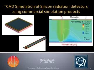
Si microstrip detectors – from the viewpoint of electric field modeling • Periodic structures with many details • Various dielectric layers (SiO2, Si with various dopants) • The geometry of dielectric layers is not precisely known (especially for SiO2) • Particular elements have orders of magnitude different dimensions (e.g. Al strips have length ~ cm, width ~ mm, thickness ~ mm) – potential problems with sharp-angled triangles • The separation of strips (~ 50 mm) is much smaller than their width Silicon Detector Workshop, Split, Croatia, 8-10 October 2012
Si microstrip detectors – modelling assumptions • Entire system could be analyzed in full (this lies within the capabilities of the Robin Hood Solver), but it is more instructive to focus on the interstrip region • the most interesting configuration of the electric fields • Observed reversed polarity signals for particles passing the interstrip region (Soić, Grassi) • Define an “elementary cell” – centered at the interstrip region • All layers of Si (differently doped) have the same dielectric constant (Capan) • Al strips can be well described as conducting plates • Various geometries for the SiO2 layer Silicon Detector Workshop, Split, Croatia, 8-10 October 2012
No SiO2 – total field strength Silicon Detector Workshop, Split, Croatia, 8-10 October 2012
No SiO2 – field strength in the x direction Silicon Detector Workshop, Split, Croatia, 8-10 October 2012
No SiO2 – field strength in the y direction Silicon Detector Workshop, Split, Croatia, 8-10 October 2012
No SiO2 – field strength in the z direction Silicon Detector Workshop, Split, Croatia, 8-10 October 2012
“Thick” SiO2 layer – start from the Si block Silicon Detector Workshop, Split, Croatia, 8-10 October 2012
“Thick” SiO2 layer – add a Si cylinder Silicon Detector Workshop, Split, Croatia, 8-10 October 2012
“Thick” SiO2 layer – make a Boolean difference of the Si plate and the cylinder Silicon Detector Workshop, Split, Croatia, 8-10 October 2012
“Thick” SiO2 layer – add a SiO2 cylinder Silicon Detector Workshop, Split, Croatia, 8-10 October 2012
“Thick” SiO2 layer – make a Boolean difference of the SiO2 cylinder and a cube Silicon Detector Workshop, Split, Croatia, 8-10 October 2012
“Thick” SiO2 layer – add Al plates Silicon Detector Workshop, Split, Croatia, 8-10 October 2012
What next? • Realistic geometry of the SiO2 layer • Dependence on the thickness of the Si (decoupling of top and bottom strips) • Spatial charge accumulated at SiO2 • Full system analysis (interference of adjacent strips) • Simulation of charge transport (big step) Silicon Detector Workshop, Split, Croatia, 8-10 October 2012
Thank you for your attention Silicon Detector Workshop, Split, Croatia, 8-10 October 2012