Nanotechnology
Nanotechnology. Important features are Nanotechnology involves research and technology development at the 1nm-to-100nm range. Nanotechnology creates and uses structures that have novel properties because of their small size.

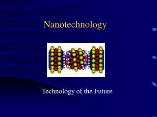
Nanotechnology
E N D
Presentation Transcript
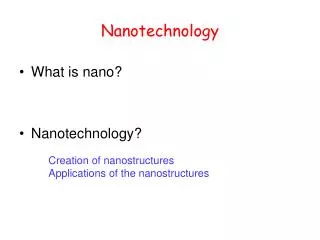
Important features are • Nanotechnology involves research and technology development at the 1nm-to-100nm range. • Nanotechnology creates and uses structures that have novel properties because of their small size. • Nanotechnology builds on the ability to control or manipulate at the atomic scale.
Effect Of Surface Body- centered cubic crystal structure Ratio of bulk molecules to surface molecules Lnbns ratio = nb /ns 1 m 8.5 x 10281.2 x 10207.3 x 108 1 mm 8.5 x 10¹⁹ 1.2 x 10147.3 x 105 1 µm 8.5 x 10¹⁰ 1.2 x 10⁸ 7.3 x 10² 100 nm 8.5 x 10⁷ 1.2 x 10⁶ 72 1 nm* 99 56 0.77 * Calculated using unit cells
Energy in Na bulk material CONTINUOUS (c) Electron in a box of length L
Usually bulk properties dominate At nanoscale • Surface effects dominate. • Quantum effects come into play. • Van der Waals forces become important. • Gravitational effectscan be ignored.
Source: European Commission. Community Research. 2004. Nanotechnology. Innovation for tomorrow’s world.
Source: Quantum Computing: “A short Course from Theory to Experiment, Joachim Stolze and Dieter Suter. Source: Quantum Computing. 2004. A Short Course from Theory to Experiment. Joachim Stoltze and Dieter Stuter.
Single-walled Carbon Nanotube d d = 0.4nm - 10nm L = ? L Lattice of covalently bonded carbon atoms
Independent Claims 1. A transistor that uses a carbon nanotube ring as a semiconductor material, the carbon nanotube ring having semiconductor characteristics. 12. A transistor that uses a carbon nanotube ring as an electrode material, the carbon nanotube ring having conductivity or semiconductor characteristics. 18. A carbon nanotube ring having p-type semiconductor characteristics. 19. A semiconductor device in which a carbon nanotube ring having p-type semiconductor characteristics is placed on an n-type semiconductor substrate thereof.
Disclosure • Detailed disclosure of ‣method to produce carbon nanotubes ‣ method to produce carbon nanotube rings from nanotubes ‣ method of fabricating transistor using nanotube ring • Basis for fall-back positions on ring diameter.
Nanotechnology in Electronics • Alternatives for transistors • Carbon nanotube transistors • Single electron transistors (SET) Memory devices • MRAM (various different approaches • Phase change RAM Photonics Nano-electromechanical system (NEMS) Fuel cells Thermo-photovoltaics Quantum computers Software
Investments • Large investments • Attracted more public funding than any other • single technology • 2003 5 to 6 Billion USD
Source:Communication from the Commission. 2004.“Towards European Strategy for Nanotechnology”.
IP Protection • Patent System • ‣ Nanotech vs .com wave • Trade Secrets • ‣ Processes
Considerations for Patent Practitioner • On practitioner level • ‣ Technology emerging, technically complex and cross- disciplinary • ‣ Practitioners not experienced • ‣ Nomenclature still developing • ‣ Lack of experience in working in multi-disciplinary teams • ‣ Case law relating to other arts. • At the Patent Offices • ‣ Emerging technology, examiners not experienced yet • ‣ Prior art collections still developing • ‣ At least in the US, no nanotechnology examining group yet - possible delays • - overly broad claims, at least initially.
Invention vs discovery • Distinction: discovery and invention, may become blurred • Discovery: ‣Carbon nanotube discovered in 1991 by Sumio Iijima • Inventions: ‣ New methods to produce carbon nanotubes consistently and economically would be patentable ‣ Applications of carbon nanotubes would be patentable • e.g. US 6,590,231B2 relating to “Transistor that uses carbon nanotube ring”
UTILITY Definition and tests — matters of national law. In ZA, the term means “effective to produce the result aimed at or promised”. In the US, 35 USC 101, an applicant must: ‣claim invention that is statutory subject matter; and ‣ show that the claimed invention is “useful” for some purpose, either explicitly or implicitly (M.P.E.P. Section 2107). Nanotechnology in its infancy — pioneering inventions Ensure at least one specific and credible utility is disclosed.
NOVELTY Invention not anticipated by prior art. Tests for anticipation and what constitutes prior art — national laws. In the US, “A claim is anticipated only if each and every element as set forth in the claim is found, either expressly or inherently described in a single prior art reference”. (Verdegaal Bros., Inc. v Union Oil Co., 814 F.2d 628, 631, 2 USPQ 2d (BNA) 1051, 1053 (Fed Cir. 1987)). Differences in size/dimensions may be important. Inherency may be a problem. Inherency can only be applied if the alleged feature would necessarily and inherently follow.
INVENTIVENESS / NON-OBVIOUSNESS Claiming something smaller — may invite an obviousness rejection. “Mere scaling……..… would not establish patentability…………”. (In re Rinehart, 531 F.2d 1048, 1053, 198 USPQ 143 (CCPA 1976)). However, may be patentable ‣ if small structure performs or functions differently; (In re Gardner v TEC Systems Inc., 725 F.2d 1338, 220 USPQ 777 (Fed.Cir. 1984)) ‣ if prior art fails to provide enabling method; (In re Hoeksema 158 USPQ 596 (CCPA 1968)). The known stalwarts: ‣ commercial success ‣ long-felt need; and ‣ unexpected results may also be relied upon.
ENABLEMENT Specification should describe the invention: ‣ sufficiently clear and complete ‣ for invention to be carried out by a person of ordinary skill in the art ‣ from info known in the art ‣ without undue experimentation. Factors that are used in US to determine whether disclosure is enabling (In re Wands): ‣ the amount of discretion or guidance presented in the spec ‣ the quantity of experimentation necessary ‣ the presence or absence of working examples ‣ the nature of the invention ‣ the state of the prior art ‣ the relative skill of those in the art ‣ the predictability or unpredictability of the art, and ‣ the breadth of the claims.
Problematic for nanotech inventions: infancy, cross-disciplines, nature, unpredictability and complexity of the technology. Extra care to include examples / embodiments, test data and adequate direction / guidance. In biotech, examiners and courts have used the enablement doctrine to narrow the scope of overly broad claims. All required information: in the specification. “Incorporation by reference” is not acceptable in the EU and JP. Person(s) of ordinary skill in the art currently ‣often Ph.D graduates ‣due to cross-disciplinary nature also group.
Nanotechnology in • South Africa (ZA) • Substantial activity at universities, research institutions, private companies and mining houses. • No formal nanotechnology strategy is in place yet. • Political transformation, R&D investment progressively decreased and reached a turning point in 1997. • R&D important for a country’s global competitiveness. • ZA missed the .com wave – Government takes nanotechnology seriously and a ZA Nanotechnology Strategy is expected to be finalised this year.
Basic nanotechnolgy research focussed on areas that are directly relevant, critical and strategic to ZA and the region. • The main drivers will be • To relieve poverty ‣ Water (membrane technology) ‣ Electricity (fuel cells) ‣ Health (drug carriers etc). • Mineral benefication ‣ gold; and ‣ titanium. • Human Resources Development
Sources: European Commission. Community Research. 2004. Nanotechnology. Innovation for tomorrow’s world. Científica Ltd. 2003. 2nd edition. The Nanotechnology Opportunity Report. European Commission. Community Research. 2004. Towards a European Strategy for Nanotechnology. Koppikar, Vivek et al., 2004. Current Trends in Nanotech Patents: A View From Inside the Patent Office. Nanotechnology Law & Business, 1(1), Article 4. Muenkel, Jonathan A. et al., Fitzpatrick Cella Harper & Scinto. Staking A Claim In The Nanoworld. Tullis Terry K. 2004. Current Intellectual Property Issues in Nanotechnology. UCLA Journal of Law of Technology, J.L. & Tech. Notes 12. Bastani B. & Fernandez D. Intellectual Property Rights in Nanotechnology. Available online: [www.iploft.com/Security(DK).pdf] 8. Halluin, Albert P. et al., 2003. Nanotechnology: The Importance Of Intellectual Property Rights In An Emerging Technology. Intellectual Property and nanotechnology. Tex Intellect Prop Law J, 11(3):220-657.
Nanotechnology 9th OPEN FORUMNovember 2005 Presented by: Adelhart Krüger DM Kisch Inc South Africa