
Cell Architecture
E N D
Presentation Transcript
04/06/06 Systems and Technology Group Cell Architecture Course code: L1T1H1-10 Cell Ecosystem Solutions Enablement 04/06/06 Course Code: L1T1H1-10 Cell Architecture © 2006 IBM Corporation Course Code: L1T1H1-10 Cell Architecture 1
04/06/06 Systems and Technology Group Class Objectives – Things you will learn ? Cell history and cell design motivation ? How cell overcomes three important limiters of contemporary microprocessor performance—power use, memory use, and processor frequency ? Cell processor organization and components – Power processor element, block diagram, PXU pipeline – Synergistic processor element, block diagram, SXU pipeline – Memory flow controller and MFC commands – Element interconnect bus, command and data topology – I/O and memory interfaces – Resource allocation management 2 Course Code: L1T1H1-10 Cell Architecture 04/06/06 © 2006 IBM Corporation Course Code: L1T1H1-10 Cell Architecture 2
04/06/06 Systems and Technology Group Class Agenda ? Cell history ? Cell highlights ? Introducing cell ? Performance over time ? Cell concept ? Microprocessor architecture trends ? Architecture motivators ? Cell synergy ? Cell features ? Cell processor components – Power processor element – Synergistic processor element – Memory flow controller – Element interconnect bus – I/O and memory interfaces – Resource allocation management References ? Jim Kahle, Cell Broadband Engine and Cell Broadband Engine Architecture Trademarks - Cell Broadband Engine ™ is a trademark of Sony Computer Entertainment, Inc. 3 Course Code: L1T1H1-10 Cell Architecture 04/06/06 © 2006 IBM Corporation Course Code: L1T1H1-10 Cell Architecture 3
04/06/06 Systems and Technology Group Cell 4 Course Code: L1T1H1-10 Cell Architecture 04/06/06 © 2006 IBM Corporation Course Code: L1T1H1-10 Cell Architecture 4
04/06/06 Systems and Technology Group Cell History ? IBM, SCEI/Sony, Toshiba Alliance formed in 2000 ? Design Center opened in March 2001 ? Based in Austin, Texas ? February 7, 2005: First technical disclosures ? May 16, 2005: First public demonstrations at E3 ? August 25, 2005: Release of technical documentation – Cell Broadband Engine Architecture documentation can be found at: ? http://www.ibm.com/developerworks/power/cell – Additional publications on Cell can be downloaded from: ? http://www.ibm.com/chips/techlib/techlib.nsf/products/Cell ? http://www.power.org/resources/devcorner/cellcorner – A paper on Cell in the IBM Journal of Research and Development can be found at: ? http://www.research.ibm.com/journal/rd/494/kahle.html 5 Course Code: L1T1H1-10 Cell Architecture 04/06/06 © 2006 IBM Corporation The first generation Cell Broadband Engine is the first member of a new family of microprocessors conforming to the Cell Broadband Engine Architecture (CBEA). The CBEA is a new architecture that extends the 64-bit PowerPC Architecture. The CBEA and the Cell Broadband Engine are the result of a collaboration between Sony, Toshiba, and IBM, known as STI, formally started in early 2001. Course Code: L1T1H1-10 Cell Architecture 5
04/06/06 Systems and Technology Group Systems and Technology Group Cell Highlights ? Supercomputer on a chip ? Multi-core microprocessor (9 cores) ? 3.2 GHz clock frequency ? 10x performance for many applications ? Digital home to distributed computing 6 6 Course Code: L1T1H1-10 Cell Architecture Course Code: L1T1H1-10 Cell Architecture 04/06/06 04/06/06 © 2006 IBM Corporation © 2005 IBM Corporation The Cell Broadband Engine is a single-chip multiprocessor with nine processors operating on a shared, coherent memory. In this respect, it extends the current trend of multi-core design in PC and server processors. Although the Cell Broadband Engine is initially intended for application in game consoles and media-rich consumer-electronics devices such as high-definition televisions, the architecture and the Cell Broadband Engine implementation have been designed to enable fundamental advances in processor performance. A much broader use of the architecture is envisioned, and that encompasses in areas such as digital media, medical imaging, seismic, financial services, and online games. Course Code: L1T1H1-10 Cell Architecture 6
04/06/06 Systems and Technology Group Introducing Cell ? Cell is an accelerator extension to Power – Built on a Power ecosystem – Used best know system practices for processor design ? Sets a new performance standard – Exploits parallelism while achieving high frequency – Supercomputer attributes with extreme floating point capabilities – Sustains high memory bandwidth with smart DMA controllers ? Designed for natural human interaction – Photo-realistic effects – Predictable real-time response – Virtualized resources for concurrent activities ? Designed for flexibility – Wide variety of application domains – Highly abstracted to highly exploitable programming models – Reconfigurable I/O interfaces – Virtual trusted computing environment for security 7 Course Code: L1T1H1-10 Cell Architecture 04/06/06 © 2006 IBM Corporation Course Code: L1T1H1-10 Cell Architecture 7
04/06/06 Systems and Technology Group Cell Concept ? Compatibility with 64b Power Architecture™ – Builds on and leverages IBM investment and community ? Increased efficiency and performance – Attacks on the “Power Wall” • Non Homogenous Coherent Multiprocessor • High design frequency @ a low operating voltage with advanced power management – Attacks on the “Memory Wall” • Streaming DMA architecture • 3-level Memory Model: Main Storage, Local Storage, Register Files – Attacks on the “Frequency Wall” • Highly optimized implementation • Large shared register files and software controlled branching to allow deeper pipelines ? Interface between user and networked world – Image rich information, virtual reality – Flexibility and security ? Multi-OS support, including RTOS / non-RTOS – Combine real-time and non-real time worlds 8 Course Code: L1T1H1-10 Cell Architecture 04/06/06 © 2006 IBM Corporation The Cell Broadband Engine overcomes three important limiters of contemporary microprocessor performance—power wall, memory wall, and processor frequency wall. The Power Wall Increasingly, microprocessor performance is limited by achievable power dissipation rather than by the number of available integrated-circuit resources (transistors and wires). Thus, the only way to significantly increase the performance of microprocessors is to improve power efficiency at about the same rate as the performance increase. One way to increase power efficiency is to differentiate between (a) processors optimized to run an operating system and control-intensive code, and (b) processors optimized to run compute intensive applications. The Cell Broadband Engine does this by providing a general-purpose PPE to run the operating system and other control-plane code, and eight SPEs specialized for computing data-rich (data-plane) applications. The Memory Wall On multi-gigahertz symmetric multiprocessors—even those with integrated memory controllers-latency to DRAM memory is currently approaching 1,000 cycles. As a result, program performance is dominated by the activity of moving data between main storage (the effective-address space that includes main memory) and the processor. Increasingly, compilers and even application writers must manage this movement of data explicitly, even though the hardware cache mechanisms are supposed to relieve them of this task. Course Code: L1T1H1-10 Cell Architecture The Cell Broadband Engine’s SPEs use two mechanisms to deal with long main-memory latencies: (a) a 3-level memory structure (main storage, local 8
04/06/06 Systems and Technology Group Frequency Increase vs Power Consumption 3.5 3 2.5 2 Realative Power Frequency 1.5 1 0.5 0 0.9 1 1.1 1.2 1.3 Voltage 9 Course Code: L1T1H1-10 Cell Architecture 04/06/06 © 2006 IBM Corporation This chart illustrates a scenario where the power dissipation increases at a much faster rate than the increase in frequency. By optimizing control-plane and data-plane processors individually, the Cell Broadband Engine mitigates the problems posed by the power, memory, and frequency limitations. The net result is a processor that, at the power budget of a conventional PC processor, can provide approximately ten-fold the peak performance of a conventional processor. Course Code: L1T1H1-10 Cell Architecture 9
04/06/06 Systems and Technology Group Systems and Technology Group Architecture Motivators ?Market Requirements ƒ Natural interaction with the system ƒ Consumer acceptable interaction ƒ Improve Experience –Ease of use –High degree of interaction –Responsive –Realism –Interconnected through network to other devices ?Holistic Design Approach ƒ Architecture ƒ Hardware implementation ƒ System structure ƒ Programming Model ?Technical Requirements ƒ Dual environment: Real time and conventional ƒ High FLOPS Computational density ƒ High parallelism ƒ Bandwidth & latency controls ƒ Realtime response ƒ Resource reservation ƒ High bandwidth Course Code: L1T1H1-10 Cell Architecture Course Code: L1T1H1-10 Cell Architecture 10 10 04/06/06 04/06/06 © 2006 IBM Corporation © 2005 IBM Corporation Course Code: L1T1H1-10 Cell Architecture 10
04/06/06 Systems and Technology Group Cell Synergy ? Cell is not a collection of different processors, but a synergistic whole – Operation paradigms, data formats and semantics consistent – Share address translation and memory protection model ? PPE for operating systems and program control ? SPE optimized for efficient data processing – SPEs share Cell system functions provided by Power Architecture – MFC implements interface to memory • Copy in/copy out to local storage ? PowerPC provides system functions – Virtualization – Address translation and protection – External exception handling ? EIB integrates system as data transport hub 11 Course Code: L1T1H1-10 Cell Architecture 04/06/06 © 2006 IBM Corporation The most distinguishing feature of the Cell Broadband Engine is that, although all processors share main storage (the effective-address space that includes main memory), their function is specialized into two types: the PowerPC Processor Element (PPE), and the Synergistic Processor Element (SPE). The Cell Broadband Engine has one PPE and eight SPEs. The first type of processor, the PPE, is a 64-bit PowerPC Architecture core. It is fully compliant with the 64-bit PowerPC Architecture and can run 32-bit and 64- bit operating systems and applications. The second type of processor, the SPE, is optimized for running compute-intensive applications, and it is not optimized for running an operating system. The SPEs are independent processors, each running its own individual application programs. Each SPE has full access to coherent shared memory, including the memory-mapped I/O space. The designation synergistic for this processor was chosen carefully because there is a mutual dependence between the PPE and the SPEs. The SPEs depend on the PPE to run the operating system, and, in many cases, the top-level control thread of an application. The PPE depends on the SPEs to provide the bulk of the application performance. The key attributes of the Cell Broadband Engine include hardware content protection, virtualization and realtime support combined with extensive single- precision floating-point capability. By extending the Power architecture with SPE having coherent DMA access to system storage and with multi operating system resource-management, CELL supports concurrent real-time and conventional Course Code: L1T1H1-10 Cell Architecture computing. With a dual-threaded PPE and 8 SPEs this implementation is capable of handling 10 simultaneous threads and over 128 outstanding memory 11
04/06/06 Systems and Technology Group Cell Features SPE ? Heterogeneous multi-core system architecture SPU SPU SPU SPU SPU SPU SPU SPU SXU SXU SXU SXU SXU SXU SXU SXU – Power Processor Element for control tasks LS LS LS LS LS LS LS LS – Synergistic Processor Elements for data-intensive processing MFC MFC MFC MFC MFC MFC MFC MFC 16B/cycle EIB (up to 96B/cycle) ? Synergistic Processor Element (SPE) consists of 16B/cycle 16B/cycle 16B/cycle (2x) PPE – Synergistic Processor Unit (SPU) PPU MIC BIC – Synergistic Memory Flow Control (MFC) PXU L1 16B/cycle L2 • Data movement and synchronization Interface to high- performance Element Interconnect Bus 32B/cycle • FlexIOTM Dual XDRTM 64-bit Power Architecture with VMX 12 Course Code: L1T1H1-10 Cell Architecture 04/06/06 © 2006 IBM Corporation The Cell Broadband Engine consists of nine processors on a single chip, all connected to each other and to external devices by a high-bandwidth, memory- coherent bus. The implementation of a first-generation CELL processor that supports multiple operating systems including Linux consists of a 64-bit power processor element (PPE) and its L2 cache, multiple synergistic processor elements (SPE) that each has its own local memory (LS), a high-bandwidth internal element interconnect bus (EIB), two configurable non-coherent I/O interfaces, a memory interface controller (MIC), and a pervasive unit that supports extensive test, monitoring, and debug functions. The PPE is the main processor. It contains a 64-bit PowerPC Architecture reduced instruction set computer (RISC) core with a traditional virtual memory subsystem. It runs an operating system, manages system resources, and is intended primarily for control processing, including the allocation and management of SPE threads. It can run legacy PowerPC Architecture software and performs well executing system-control code. It supports both the PowerPC instruction set and the Vector/SIMD Multimedia Extension instruction set. The eight SPEs are SIMD processors optimized for data-rich operations allocated to them by the PPE. Each of these identical elements contains a RISC core, 256-KB, software-controlled local store for instructions and data, and a Course Code: L1T1H1-10 Cell Architecture large (128-bit, 128-entry) unified register file. The SPEs support a special SIMD instruction set, and they rely on asynchronous DMA transfers through the 12
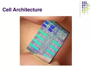
04/06/06 Systems and Technology Group Cell Broadband Engine – 235mm2 13 Course Code: L1T1H1-10 Cell Architecture 04/06/06 © 2006 IBM Corporation This chart depicts a die micrograph of the cell microprocessor chip. The die shows roughly 234M transistors from 17 physical entities and 580k repeaters and 1.4M nets implemented in 90nm SOI technology with 8 levels of copper interconnects and one local interconnect layer. At the center of the chip is the EIB composed of four 128b data rings plus a 64b tag operated at half the processor clock rate. The wires are arranged in groups of four, interleaved with GND and VDD shields twisted at the center to reduce coupling noise on the two unshielded wires. To ensure signal integrity, over 50% of global nets are engineered with 32k repeaters. The SoC uses 2965 C4s with four regions of different row-column pitches attached to a low-cost organic package. This structure supports 15 separate power domains on the chip, many of which overlap physically on the die. The processor element design, power and clock grids, global routing, and chip assembly support a modular design in a building-block-like construction. Course Code: L1T1H1-10 Cell Architecture 13
04/06/06 Systems and Technology Group Cell Processor Components In the Beginning – the solitary Power Processor Power Processor Element (PPE): • General purpose, 64-bit RISC processor (PowerPC AS 2.0.2) • 2-Way hardware multithreaded • L1 : 32KB I ; 32KB D • L2 : 512KB • Coherent load / store • VMX-32 • Realtime Controls – Locking L2 Cache & TLB – Software / hardware managed TLB – Bandwidth / Resource Reservation – Mediated Interrupts 96 Byte/Cycle NCU Power Core (PPE) L2 Cache Element Interconnect Bus Custom Designed – for high frequency, space, and power efficiency Element Interconnect Bus (EIB): • Four 16 byte data rings supporting multiple simultaneous transfers per ring • 96Bytes/cycle peak bandwidth • Over 100 outstanding requests 04/06/06 © 2006 IBM Corporation Course Code: L1T1H1-10 Cell Architecture 14 .1 The PowerPC Processor Element (PPE) is a general-purpose, dual-threaded, 64-bit RISC processor that conforms to the PowerPC Architecture, version 2.02, with the Vector/SIMD Multimedia Extension. Programs written for the PowerPC 970 processor, for example, should run on the Cell Broadband Engine without modification. The PPE consists of two main units, the PowerPC Processor Unit (PPU) and the Storage Subsystem. The PPE is responsible for overall control of the system including instruction control and execution. It runs the operating systems for all applications running on the Cell Broadband Engine. The PPU includes the full set of 64-bit PowerPC registers, 32 128-bit vector multimedia registers, a 32-KB level 1 (L1) instruction cache, a 32-KB level 1 (L1) data cache, an instruction-control unit, a load and store unit, a fixed-point integer unit, a floating-point unit, a vector unit, a branch unit, and a virtual- memory management unit. The L2 cache and the address-translation caches use replacement- management tables that allow software to control use of the caches. This software control over cache resources is especially useful for real-time programming. Course Code: L1T1H1-10 Cell Architecture storage and I/O through the EIB. The EIB is a 4-ring structure (two clockwise The PPE and SPEs communicate coherently with each other and with main 14
04/06/06 Systems and Technology Group Local Store Cell Processor Components Local Store SPU SPU Synergistic Processor Element (SPE): • Provides the computational performance • Simple RISC User Mode Architecture – Dual issue VMX-like – Graphics SP-Float – IEEE DP-Float • Dedicated resources: unified 128x128-bit RF, 256KB Local Store • Dedicated DMA engine: Up to 16 outstanding requests AUC AUC MFC MFC N N 96 Byte/Cycle AUC Local Store MFC SPU N NCU N SPU MFC Local Store AUC Power Core (PPE) AUC Local Store L2 Cache MFC SPU N SPU MFC N Local Store AUC Element Interconnect Bus Memory Management & Mapping • SPE Local Store aliased into PPE system memory • MFC/MMU controls / protects SPE DMA accesses – Compatible with PowerPC Virtual Memory Architecture – SW controllable using PPE MMIO • DMA 1,2,4,8,16,128 -> 16Kbyte transfers for I/O access • Two queues for DMA commands: Proxy & SPU N N MFC MFC AUC AUC Local Store Local Store SPU SPU 04/06/06 © 2006 IBM Corporation Course Code: L1T1H1-10 Cell Architecture 15 .1 The eight SPEs are SIMD processors, each of these identical elements contains a RISC core, 256-KB, software-controlled local store for instructions and data, and a large (128-bit, 128-entry) unified register file. The SPEs are not intended to run an operating system. Each of the eight Synergistic Processor Elements (SPEs) contains two main units, the Synergistic Processor Unit (SPU) and the Memory Flow Controller (MFC). The MFC contains a DMA controller that supports DMA transfers. Programs running on the SPU, the PPE, or another SPU, use the MFC’s DMA transfers to move instructions and data between the SPU’s LS and main storage. (Main storage is the effective-address space that includes main memory, other SPEs’ LS, and memory-mapped registers such as memory-mapped I/O [MMIO] registers.) Each DMA transfer can be up to 16 KB in size. However, only the MFC’s associated SPU can issue DMA-list commands. These can represent up to 2,048 DMA transfers, each one up to 16 KB in size. DMA transfers are coherent with respect to main storage. Virtual-memory address translation information is provided to each MFC by the operating system running on the PPE. Course Code: L1T1H1-10 Cell Architecture 15
04/06/06 Systems and Technology Group 25 GB/sec XDR DRAM Local Store Cell Processor Components Local Store SPU SPU Broadband Interface Controller (BIC): ? Provides a wide connection to external devices ? Two configurable interfaces (60GB/s @ 5Gbps) – Configurable number of bytes – Coherent (BIF) and / or I/O (IOIFx) protocols ? Supports two virtual channels per interface ? Supports multiple system configurations AUC AUC MFC MFC MIC N N 96 Byte/Cycle AUC Local Store MFC SPU N NCU N SPU MFC Local Store AUC Power Core (PPE) AUC Local Store L2 Cache MFC SPU N SPU MFC N Local Store AUC Memory Interface Controller (MIC): • Dual XDRTMcontroller (25.6GB/s @ 3.2Gbps) • ECC support • Suspend to DRAM support Element Interconnect Bus N N IOIF1 IOIF0 MFC MFC AUC AUC 5 GB/sec Local Store Local Store Southbridge I/O SPU SPU 20 GB/sec BIF or IOIF0 04/06/06 © 2006 IBM Corporation Course Code: L1T1H1-10 Cell Architecture 16 .1 The Cell Broadband Engine Interface (BEI) supports I/O interfacing. It includes a Broadband Interface Controller (BIC), I/O Controller (IOC), and Internal Interrupt Controller (IIC). It manages data transfers between the EIB and I/O devices and provides I/O address translation and command processing. The BEI supports two Rambus FlexIO interfaces (channels). One of the two interfaces (IOIF1) supports only a non-coherent I/O Interface (IOIF) protocol, which is suitable for I/O devices. The other interface (IOIF0, also called BIF/IOIF0) is software-selectable between the non-coherent protocol and the fully coherent Broadband Interface (BIF) protocol—the EIB’s native internal protocol—which coherently extends the EIB to another device that can be another CBE processor. Thus, a CBE processor is designed to be ganged coherently with other CBE processors to produce a cluster. The Memory Interface Controller provides the interface between the EIB and main storage. It supports two Rambus Extreme Data Rate (XDR) I/O (XIO) memory channels and memory accesses on each channel of 1-8, 16, 32, 64, or 128 bytes. Course Code: L1T1H1-10 Cell Architecture 16
04/06/06 Systems and Technology Group 25 GB/sec XDR DRAM Local Store Cell Processor Components Local Store SPU SPU Internal Interrupt Controller (IIC) ? Handles SPE Interrupts ? Handles External Interrupts – From Coherent Interconnect – From IOIF0 or IOIF1 ? Interrupt Priority Level Control ? Interrupt Generation Ports for IPI ? Duplicated for each PPE hardware thread AUC AUC MFC MFC MIC N N 96 Byte/Cycle AUC Local Store MFC SPU N NCU N SPU MFC Local Store AUC Power Core (PPE) AUC Local Store L2 Cache MFC SPU N SPU MFC N Local Store AUC IIC IOT Element Interconnect Bus N N IOIF1 IOIF0 MFC MFC AUC AUC I/O Bus Master Translation (IOT) ? Translates Bus Addresses to System Real Addresses ? Two Level Translation – I/O Segments (256 MB) – I/O Pages (4K, 64K, 1M, 16M byte) ? I/O Device Identifier per page for LPAR ? IOST and IOPT Cache – hardware / software managed 5 GB/sec Local Store Local Store Southbridge I/O SPU SPU 20 GB/sec BIF or IOIF0 04/06/06 © 2006 IBM Corporation Course Code: L1T1H1-10 Cell Architecture 17 .1 The interrupt controller handles SPE interrupts and external interrupts from coherent interconnect and from IO channels. The IIC component manages the priority of the interrupts presented to the PPEs. The main purpose of the IIC is to allow interrupts from the other components in the processor to be handled without using the main system interrupt controller. The IIC is really a second level controller. It is intended to handle all interrupts internal to a CBEA-compliant processor or within a multiprocessor system of CBEA-compliant processors. The system interrupt controller will typically handle all interrupts external to the CBEA-compliant processor. In a CBEA-compliant system, software must first check the IIC to determine if the interrupt was sourced from an external system interrupt controller. The IIC is not intended to replace the main system interrupt controller for handling interrupts from all I/O devices. Course Code: L1T1H1-10 Cell Architecture 17
04/06/06 Systems and Technology Group 25 GB/sec XDR DRAM Local Store Cell Processor Components Local Store SPU SPU Token Manager (TKM): ? Bandwidth / Resource Reservation for shared resources ? Optionally enabled for RT tasks or LPAR ? Multiple Resource Allocation Groups (RAGs) ? Generates access tokens at configurable rate for each allocation group – 1 per each memory bank (16 total) – 2 for each IOIF (4 total) ? Requestors assigned RAG ID by OS / hypervisor – Each SPE – PPE L2 / NCU – IOIF 0 Bus Master – IOIF 1 Bus Master ? Priority order for using another RAGs unused tokens ? Resource over committed warning interrupt AUC AUC MFC MFC MIC N N 96 Byte/Cycle TKM AUC Local Store MFC SPU N NCU N SPU MFC Local Store AUC Power Core (PPE) AUC Local Store L2 Cache MFC SPU N SPU MFC N Local Store AUC IIC IOT Element Interconnect Bus N N IOIF1 IOIF0 MFC MFC AUC AUC 5 GB/sec Local Store Local Store Southbridge I/O SPU SPU 20 GB/sec BIF or IOIF0 04/06/06 © 2006 IBM Corporation Course Code: L1T1H1-10 Cell Architecture 18 The Token Management Unit is a part of the Element Interconnect Bus (EIB) that software can program to regulate the rate at which particular devices are allowed to make EIB command requests. Course Code: L1T1H1-10 Cell Architecture 18
04/06/06 Systems and Technology Group Power Processor Element ? PPE handles operating system and control tasks – 64-bit Power ArchitectureTMwith VMX – In-order, 2-way hardware simultaneous multi-threading (SMT) – Coherent Load/Store with 32KB I & D L1 and 512KB L2 19 Course Code: L1T1H1-10 Cell Architecture 04/06/06 © 2006 IBM Corporation Course Code: L1T1H1-10 Cell Architecture 19
04/06/06 Systems and Technology Group PPE BLOCK DIAGRAM Pre-Decode 8 Fetch Control Threads alternate fetch and dispatch cycles L1 Instruction Cache Thread A Thread B L2 Interface 4 4 Branch Scan SMT Dispatch (Queue) Microcode 2 1 Decode Dependency Issue 2 Thread A L1 Data Cache Thread B Thread A 1 1 1 VMX/FPU Issue (Queue) 2 1 Branch Execution Unit Load/Store Unit Fixed-Point Unit 1 1 1 VMX VMX FPU FPU Completion/Flush Load/Store/ Permute Arith./Logic Unit Arith/Logic Unit Load/Store VMX Completion FPU Completion 04/06/06 © 2006 IBM Corporation Course Code: L1T1H1-10 Cell Architecture 20 Course Code: L1T1H1-10 Cell Architecture 20
04/06/06 Systems and Technology Group PXU PIPELINE FRONT END Microcode MC4 MC3 MC10 MC9 MC1 MC2 ... MC11 IC1 IC2 Instruction Cache and Buffer IC3 IC4 IB1 IS3 IB2 ID1 ID2 ID3 IS1 IS2 Instruction Decode and Issue BP1 BP2 BP3 BP4 Branch Prediction PPE PIPELINE BACK END IC Instruction Cache IB Instruction Buffer BP Branch Prediction MC Microcode ID Instruction Decode IS Instruction Issue DLY Delay Stage RF Register File Access EX Execution WB Write Back Branch Instruction DL Y EX4 DL Y DL Y RF2 EX1 EX2 EX3 IBZ RF1 IC0 Fixed Point Unit Instruction DL Y DL Y DL Y EX5 RF1 RF2 WB EX1 EX2 EX3 EX4 Load/Store Instruction EX6 EX2 EX5 RF1 RF2 EX1 EX3 EX4 EX8 EX7 WB 04/06/06 © 2006 IBM Corporation Course Code: L1T1H1-10 Cell Architecture 21 Course Code: L1T1H1-10 Cell Architecture 21
04/06/06 Systems and Technology Group Synergistic Processor Element ? SPE provides computational performance – Dual issue, up to 16-way 128-bit SIMD – Dedicated resources: 128 128-bit RF, 256KB Local Store – Each can be dynamically configured to protect resources – Dedicated DMA engine: Up to 16 outstanding requests 22 Course Code: L1T1H1-10 Cell Architecture 04/06/06 © 2006 IBM Corporation The SPU implements a new instruction set architecture (ISA). It supports dual issue and up to 16-way 128-bit SIMD. The main characteristics of this architecture are: • Load-and-store architecture with sequential semantics, using a set of 128 registers, each of which is 128 bits wide. • Single-instruction, multiple-data (SIMD) capability – Sixteen 8-bit integers – Eight 16-bit integers – Four 32-bit integer or four single-precision floating-point values – Two double-precision floating point • Load-and-store access to an associated local storage. • Channel input/output for MFC control (used for external data access). Course Code: L1T1H1-10 Cell Architecture 22
04/06/06 Systems and Technology Group SPE Highlights ? RISC like organization – 32 bit fixed instructions – Clean design – unified Register file ? User-mode architecture – No translation/protection within SPU – DMA is full Power Arch protect/x-late ? VMX-like SIMD dataflow – Broad set of operations (8 / 16 / 32 Byte) – Graphics SP-Float – IEEE DP-Float ? Unified register file – 128 entry x 128 bit ? 256KB Local Store – Combined I & D – 16B/cycle L/S bandwidth – 128B/cycle DMA bandwidth LS DP SFP LS FXU EVN FWD LS FXU ODD CONTROL GPR LS CHANNEL DMA SMM ATO RTB BEB SBI 14.5mm2(90nm SOI) 23 Course Code: L1T1H1-10 Cell Architecture 04/06/06 © 2006 IBM Corporation The Synergistic Processor Element (SPE) is the first implementation of a new processor architecture designed to accelerate media and streaming workloads. Area and power efficiency are important enablers for multi-core designs that take advantage of parallelism in applications . The architecture reduces area and power by solving scheduling problems such as data fetch and branch prediction in software. SPE provides an isolated execution mode that restricts access to certain resources to validated programs. The focus on efficiency comes at the cost of multi-user operating system support. SPE load and store instructions are performed within a local address space, not in system address space. The local address space is untranslated, unguarded and non-coherent with respect to the system address space and is serviced by the local store (LS). Loads, stores and instruction fetch complete without exception, greatly simplifying the core design. The LS is a fully pipelined, single-ported, 256kb SRAM that supports quadword (16B) or line (128B) access. The SPE is a SIMD processor programmable in high level languages such as C or C++ with intrinsics. Most instructions process 128b operands, divided into four 32b words. The 128b operands are stored in a 128-entry-unified-register file used for integer, floating point and conditional operations. The large register file facilitates deep unrolling to fill execution pipelines. Course Code: L1T1H1-10 Cell Architecture Data is transferred to and from the LS in 1024b lines by the SPE DMA engine 23
04/06/06 Systems and Technology Group What is a Synergistic Processor? (and why is it efficient?) ? Local Store “is” large 2ndlevel register file / private instruction store instead of cache – Asynchronous transfer (DMA) to shared memory Frontal attack on the Memory Wall ? Media Unit turned into a Processor – LS DP – Unified (large) Register File SFP SPU 128 entry x 128 bit ? Media & Compute optimized – LS FXU EVN FWD – One context LS FXU ODD – SIMD architecture CONTROL GPR LS CHANNEL DMA SMM ATO SMF RTB BEB SBI 04/06/06 © 2006 IBM Corporation Course Code: L1T1H1-10 Cell Architecture 24 The intent of the SPU is to fill a void between general-purpose processors and special-purpose hardware. Where general-purpose processors aim to achieve the best average performance on a broad set of applications, and special-purpose hardware aims to achieve the best performance on a single application, the SPU aims to achieve leadership performance on critical workloads for game, media, and broadband systems. Course Code: L1T1H1-10 Cell Architecture 24
04/06/06 Systems and Technology Group SPU Detail Synergistic Processor Element (SPE) ? User-mode architecture SPU Units: – Simple (FXU even) L S – No translation/protection within SPE D P • • • Add/Compare Rotate Logical, Count Leading Zero S F P DMA is full PowerPC protect/xlate Direct programmer control – L S ? F X U E V N – Permute (FXU odd) – DMA/DMA-list F W D • • Permute Table-lookup – Branch hint L S F X U O D D ? CONTROL VMX-like SIMD dataflow – FPU (Single / Double Precision) – Graphics SP-Float – Control (SCN) G P R – No saturate arith, some byte • Dual Issue, Load/Store, ECC Handling L S IEEE DP-Float (BlueGene-like) Unified register file – – Channel (SSC) – Interface to MFC C H A N N E L ? – Register File (GPR/FWD) D M A – 128 entry x 128 bit S M M A T O ? 256KB Local Store – Combined I & D R T B BEB S B I – 16B/cycle L/S bandwidth 128B/cycle DMA bandwidth Memory Flow Control (MFC) – ? SPU Latencies – Simple fixed point - 2 cycles* – Complex fixed point - 4 cycles* – Load - 6 cycles* • Local store size = 256 KB – Single-precision (ER) float - 6 cycles* – Integer multiply - 7 cycles* – Branch miss - 20 cycles • No penalty if correctly hinted – DP (IEEE) float - 13 cycles* • Partially pipelined – Enqueue DMA Command - 20 cycles* 04/06/06 © 2006 IBM Corporation Course Code: L1T1H1-10 Cell Architecture 25 Course Code: L1T1H1-10 Cell Architecture 25
04/06/06 Systems and Technology Group SPE BLOCK DIAGRAM Floating-Point Unit Permute Unit Fixed-Point Unit Load-Store Unit Branch Unit Local Store (256kB) Single Port SRAM Channel Unit Result Forwarding and Staging Register File Instruction Issue Unit / Instruction Line Buffer 128B Read 128B Write On-Chip Coherent Bus DMA Unit 8 Byte/Cycle 16 Byte/Cycle 64 Byte/Cycle 128 Byte/Cycle 04/06/06 © 2006 IBM Corporation Course Code: L1T1H1-10 Cell Architecture 26 Instructions are fetched from the LS in 32 4B groups. Fetch groups are aligned to 64B boundaries to improve the effective instruction fetch bandwidth. 3.5 fetched lines are stored in the instruction line buffer (ILB). One-half line holds instructions while they are sequenced into the issue logic; as another line holds the single entry software managed branch target buffer (SMBTB) and two lines are used for inline prefetching. Efficient software manages branches in three ways: it replaces branches with bit-wise select instructions; it arranges for the common case to be inline; it inserts branch hint instructions to identify branches and load the probable targets into the SMBTB. The SPE can issue up to two instructions per cycle to seven execution units organized in two execution pipelines. Instructions are issued in program order. Instruction fetch sends double word address-aligned instruction pairs to the issue logic. Instruction pairs are issued if the first instruction (from an even address) is routed to an even pipe unit and the second instruction to an odd pipe unit. Loads and stores wait in the issue stage for an available LS cycle. Issue control and distribution require three cycles. The pipeline diagram shows operands that are fetched either from the register file or forward network. The register file has six read ports, two write ports, 128 entries of 128b each and is accessed in two cycles. Register file data is sent Course Code: L1T1H1-10 Cell Architecture directly to unit operand latches. Results produced by functional units are held in the forward macro until they are committed and available from the register file. 26
04/06/06 Systems and Technology Group SXU PIPELINE FRONT END IF3 IF4 IF5 IB1 IB2 ID1 ID2 ID3 IF1 IF2 IS1 IS2 SPE PIPELINE BACK END Branch Instruction RF1 RF2 IF Instruction Fetch IB Instruction Buffer ID Instruction Decode IS Instruction Issue RF Register File Access EX Execution WB Write Back Permute Instruction EX1 EX2 EX3 EX4 WB Load/Store Instruction EX6 EX2 EX5 EX1 EX3 EX4 WB Fixed Point Instruction EX1 EX2 WB Floating Point Instruction EX1 EX3 EX4 EX5 EX6 WB EX2 04/06/06 © 2006 IBM Corporation Course Code: L1T1H1-10 Cell Architecture 27 This chart details the execution units in the SPU pipeline. Unit to pipeline assignment maximizes performance given the rigid issue rules. Simple fixed point, floating point and load results are bypassed directly from the unit output to input operands reducing result latency. Other results are sent to the forward macro where they are distributed one cycle later. Course Code: L1T1H1-10 Cell Architecture 27
04/06/06 Systems and Technology Group MFC Detail Memory Flow Control System •DMA Unit •LS <-> LS, LS<-> Sys Memory, LS<-> I/O Transfers •8 PPE-side Command Queue entries •16 SPU-side Command Queue entries •MMU similar to PowerPC MMU •8 SLBs, 256 TLBs •4K, 64K, 1M, 16M page sizes •Software/HW page table walk •PT/SLB misses interrupt PPE •Atomic Cache Facility •4 cache lines for atomic updates •2 cache lines for cast out/MMU reload •Up to 16 outstanding DMA requests in BIU •Resource / Bandwidth Management Tables •Token Based Bus Access Management •TLB Locking Local Store SPU SPC Legend: Data Bus Snoop Bus Control Bus Xlate Ld/St MMIO DMA Engine DMA Queue Atomic Facility MMU RMT Bus I/F Control MMIO Isolation Mode Support (Security Feature) ? Hardware enforced “isolation” – SPU and Local Store not visible (bus or jtag) Small LS “untrusted area” for communication area Secure Boot – ? – Chip Specific Key Decrypt/Authenticate Boot code “Secure Vault” – Runtime Isolation Support – ? – Isolate Load Feature – Isolate Exit Feature 04/06/06 © 2006 IBM Corporation Course Code: L1T1H1-10 Cell Architecture 28 Course Code: L1T1H1-10 Cell Architecture 28
04/06/06 Systems and Technology Group Per SPE Resources (PPE Side) Problem State Privileged 2 State (OS or Hypervisor) Privileged 1 State (OS) 4K Physical Page Boundary 4K Physical Page Boundary 4K Physical Page Boundary 8 Entry MFC Command Queue Interface DMA Command and Queue Status DMA Tag Status Query Mask DMA Tag Status 32 bit Mailbox Status and Data from SPU 32 bit Mailbox Status and Data to SPU 4 deep FIFO Signal Notification 1 Signal Notification 2 SPU Run Control SPU Next Program Counter SPU Execution Status SPU Master Run Control SPU ID SPU ECC Control SPU ECC Status SPU ECC Address SPU 32 bit PU Interrupt Mailbox MFC Interrupt Mask MFC Interrupt Status MFC DMA Privileged Control MFC Command Error Register MFC Command Translation Fault Register MFC SDR (PT Anchor) MFC ACCR (Address Compare) MFC DSSR (DSI Status) MFC DAR (DSI Address) MFC LPID (logical partition ID) MFC TLB Management Registers SPU Privileged Control SPU Channel Counter Initialize SPU Channel Data Initialize SPU Signal Notification Control SPU Decrementer Status & Control MFC DMA Control MFC Context Save / Restore Registers SLB Management Registers 4K Physical Page Boundary 4K Physical Page Boundary Optionally Mapped 256K Local Store Optionally Mapped 256K Local Store 04/06/06 © 2006 IBM Corporation Course Code: L1T1H1-10 Cell Architecture 29 Course Code: L1T1H1-10 Cell Architecture 29
04/06/06 Systems and Technology Group Per SPE Resources (SPU Side) SPU Direct Access Resources SPU Indirect Access Resources (via EA Addressed DMA) 128 - 128 bit GPRs External Event Status (Channel 0) Decrementer Event Tag Status Update Event DMA Queue Vacancy Event SPU Incoming Mailbox Event Signal 1 Notification Event Signal 2 Notification Event Reservation Lost Event External Event Mask (Channel 1) External Event Acknowledgement (Channel 2) Signal Notification 1 (Channel 3) Signal Notificaiton 2 (Channel 4) Set Decrementer Count (Channel 7) Read Decrementer Count (Channel 8) 16 Entry MFC Command Queue Interface (Channels 16-21) DMA Tag Group Query Mask (Channel 22) Request Tag Status Update (Channel 23) Immediate Conditional - ALL Conditional - ANY Read DMA Tag Group Status (Channel 24) DMA List Stall and Notify Tag Status (Channel 25) DMA List Stall and Notify Tag Acknowledgement (Channel 26) Lock Line Command Status (Channel 27) Outgoing Mailbox to PU (Channel 28) Incoming Mailbox from PU (Channel 29) Outgoing Interrupt Mailbox to PU (Channel 30) System Memory Memory Mapped I/O This SPU Local Store Other SPU Local Store Other SPU Signal Registers Atomic Update (Cacheable Memory) 04/06/06 © 2006 IBM Corporation Course Code: L1T1H1-10 Cell Architecture 30 Course Code: L1T1H1-10 Cell Architecture 30
04/06/06 Systems and Technology Group Memory Flow Controller Commands DMA Commands Put - Transfer from Local Store to EA space Puts - Transfer and Start SPU execution Putr - Put Result - (Arch. Scarf into L2) Putl - Put using DMA List in Local Store Putrl - Put Result using DMA List in LS (Arch) Get - Transfer from EA Space to Local Store Gets - Transfer and Start SPU execution Getl - Get using DMA List in Local Store Sndsig - Send Signal to SPU Command Modifiers: <f,b> f: Embedded Tag Specific Fence Command will not start until all previous commands in same tag group have completed b: Embedded Tag Specific Barrier Command and all subsiquent commands in same tag group will not start until previous commands in same tag group have completed Command Parameters LSA - Local Store Address (32 bit) EA - Effective Address (32 or 64 bit) TS - Transfer Size (16 bytes to 16K bytes) LS - DMA List Size (8 bytes to 16 K bytes) TG - Tag Group(5 bit) CL - Cache Management / Bandwidth Class Synchronization Commands Lockline (Atomic Update) Commands: getllar - DMA 128 bytes from EA to LS and set Reservation putllc - Conditionally DMA 128 bytes from LS to EA putlluc - Unconditionally DMA 128 bytes from LS to EA barrier - all previous commands complete before subsiquent commands are started mfcsync - Results of all previous commands in Tag group are remotely visible mfceieio - Results of all preceding Puts commands in same group visible with respect to succeeding Get commands SL1 Cache Management Commands sdcrt - Data cache region touch (DMA Get hint) sdcrtst - Data cache region touch for store (DMA Put hint) sdcrz - Data cache region zero sdcrs - Data cache region store sdcrf - Data cache region flush 04/06/06 © 2006 IBM Corporation Course Code: L1T1H1-10 Cell Architecture 31 Course Code: L1T1H1-10 Cell Architecture 31
04/06/06 Systems and Technology Group SPE Structure ? Scalar processing supported on data-parallel substrate – All instructions are data parallel and operate on vectors of elements – Scalar operation defined by instruction use, not opcode • Vector instruction form used to perform operation ? Preferred slot paradigm – Scalar arguments to instructions found in “preferred slot” – Computation can be performed in any slot 32 Course Code: L1T1H1-10 Cell Architecture 04/06/06 © 2006 IBM Corporation Course Code: L1T1H1-10 Cell Architecture 32
04/06/06 Systems and Technology Group Register Scalar Data Layout ? Preferred slot in bytes 0-3 – By convention for procedure interfaces – Used by instructions expecting scalar data • Addresses, branch conditions, generate controls for insert 33 Course Code: L1T1H1-10 Cell Architecture 04/06/06 © 2006 IBM Corporation Course Code: L1T1H1-10 Cell Architecture 33
04/06/06 Systems and Technology Group Element Interconnect Bus ? EIB data ring for internal communication – Four 16 byte data rings, supporting multiple transfers – 96B/cycle peak bandwidth – Over 100 outstanding requests 34 Course Code: L1T1H1-10 Cell Architecture 04/06/06 © 2006 IBM Corporation Course Code: L1T1H1-10 Cell Architecture 34
04/06/06 Systems and Technology Group Element Interconnect Bus – Command Topology ? ? ? ? ? ? “Address Concentrator” tree structure minimizes wiring resources Single serial command reflection point (AC0) Address collision detection and prevention Fully pipelined Content –aware round robin arbitration Credit-based flow control SPE1 SPE3 SPE5 SPE7 PPE IOIF1 CMD CMD CMD CMD A C 3 A C 2 A C 1 A C 2 CMD CMD AC0 CMD CMD CMD CMD CMD Off-chip AC0 BIF/IOIF0 MIC SPE0 SPE2 SPE6 SPE4 35 Course Code: L1T1H1-10 Cell Architecture 04/06/06 © 2006 IBM Corporation Course Code: L1T1H1-10 Cell Architecture 35
04/06/06 Systems and Technology Group Element Interconnect Bus - Data Topology ? Four 16B data rings connecting 12 bus elements – Two clockwise / Two counter-clockwise ? ? Physically overlaps all processor elements Central arbiter supports up to three concurrent transfers per data ring – Two stage, dual round robin arbiter ? Each element port simultaneously supports 16B in and 16B out data path – Ring topology is transparent to element data interface SPE1 SPE3 SPE5 SPE7 PPE IOIF1 16B 16B 16B 16B 16B 16B 16B 16B 16B 16B 16B 16B Data Arb 16B 16B 16B 16B 16B 16B 16B 16B 16B 16B 16B 16B BIF/IOIF0 MIC SPE0 SPE2 SPE6 SPE4 36 Course Code: L1T1H1-10 Cell Architecture 04/06/06 © 2006 IBM Corporation Course Code: L1T1H1-10 Cell Architecture 36
04/06/06 Systems and Technology Group Internal Bandwidth Capability ? Each EIB Bus data port supports 25.6GBytes/sec* in each direction ? The EIB Command Bus streams commands fast enough to support 102.4 GB/sec for coherent commands, and 204.8 GB/sec for non-coherent commands. ? The EIB data rings can sustain 204.8GB/sec for certain workloads, with transient rates as high as 307.2GB/sec between bus units Despite all that available bandwidth… * The above numbers assume a 3.2GHz core frequency – internal bandwidth scales with core frequency 37 Course Code: L1T1H1-10 Cell Architecture 04/06/06 © 2006 IBM Corporation Course Code: L1T1H1-10 Cell Architecture 37
04/06/06 Systems and Technology Group Example of eight concurrent transactions PPE PPE SPE1 SPE1 SPE3 SPE3 SPE5 SPE5 IOIF1 IOIF1 SPE7 SPE7 Ramp Ramp Ramp Ramp Ramp Ramp Ramp 7 Ramp 8 Ramp 9 Ramp 10 Ramp 11 6 7 8 9 10 11 Controller Controller Controller Controller Controller Controller Controller Controller Controller Controller Controller Data Arbiter Controller Controller Controller Controller Controller Controller Controller Controller Controller Controller Controller Controller Controller Controller Controller Controller Controller Ramp 9 Ramp Ramp 7 Ramp Ramp 8 Ramp Ramp 11 Ramp Ramp Ramp 10 Ramp 2 Ramp 4 3 0 5 1 Ramp 4 Ramp 3 Ramp 2 Ramp 1 Ramp 0 5 BIF / IOIF1 IOIF0 IOIF1 BIF / MIC PPE MIC SPE0 SPE1 SPE0 SPE2 SPE3 SPE2 SPE4 SPE5 SPE4 SPE6 SPE7 SPE6 Ring1 Ring3 Ring0 Ring2 controls 38 Course Code: L1T1H1-10 Cell Architecture 04/06/06 © 2006 IBM Corporation Course Code: L1T1H1-10 Cell Architecture 38
04/06/06 Systems and Technology Group Resource Allocation Management ? Optional facility used to minimize over-allocation effects of critical resources – Independent but complementary function to the EIB – Critical (managed) resource’s time is distributed among groups of requestors ? Managed resources include: – Rambus XDRTMDRAM memory banks (0 to 15) – BIF/IOIF0 Inbound and BIF/IOIF0 Outbound – IOIF1 Inbound and IOIF1 Outbound ? Requestors Allocated to Four Resource Allocation Groups (RAG) – 17 requestors – PPE, SPEs, I/O Inbound (4 VCs), I/O Outbound (4 VCs) ? Central Token Manager controller – Requestors ask permission to issue EIB commands to managed resources – Tokens granted across RAGs allow requestor access to issue command to the EIB – Round robin allocation within RAG – Dynamic software configuration of the Token Manager to adjust token allocation rates for varying workloads – Multi-level hardware feedback from managed resource congestion to throttle token allocation 39 Course Code: L1T1H1-10 Cell Architecture 04/06/06 © 2006 IBM Corporation Course Code: L1T1H1-10 Cell Architecture 39
04/06/06 Systems and Technology Group I/O and Memory Interfaces ? I/O Provides wide bandwidth – Dual XDRTMcontroller (25.6GB/s @ 3.2Gbps) – Two configurable interfaces (76.8GB/s @6.4Gbps) • Configurable number of Bytes • Coherent or I/O Protection – Allows for multiple system configurations 40 Course Code: L1T1H1-10 Cell Architecture 04/06/06 © 2006 IBM Corporation Course Code: L1T1H1-10 Cell Architecture 40
04/06/06 Systems and Technology Group Cell BE Processor Can Support Many Systems ? Game console systems ? Blades ? HDTV ? Home media servers ? Supercomputers XDRtm XDRtm XDRtm XDRtm Cell BE Processor Cell BE Processor IOIF BIF IOIF XDRtm XDRtm XDRtm XDRtm XDRtm XDRtm Cell BE Processor Cell BE Processor IOIF IOIF BIF BIF SW IOIF IOIF Processor Processor Cell BE Cell BE Cell BE Processor IOIF0 IOIF1 XDRtm XDRtm XDRtm XDRtm 41 Course Code: L1T1H1-10 Cell Architecture 04/06/06 © 2006 IBM Corporation Course Code: L1T1H1-10 Cell Architecture 41
04/06/06 Systems and Technology Group Summary ? Cell ushers in a new era of leading edge processors optimized for digital media and entertainment ? Desire for realism is driving a convergence between supercomputing and entertainment ? New levels of performance and power efficiency beyond what is achieved by PC processors ? Responsiveness to the human user and the network are key drivers for Cell ? Cell will enable entirely new classes of applications, even beyond those we contemplate today 42 Course Code: L1T1H1-10 Cell Architecture 04/06/06 © 2006 IBM Corporation Course Code: L1T1H1-10 Cell Architecture 42
04/06/06 Systems and Technology Group (c) Copyright International Business Machines Corporation 2005. All Rights Reserved. Printed in the United Sates April 2005. The following are trademarks of International Business Machines Corporation in the United States, or other countries, or both. IBM IBM Logo Power Architecture Other company, product and service names may be trademarks or service marks of others. All information contained in this document is subject to change without notice. The products described in this document are NOT intended for use in applications such as implantation, life support, or other hazardous uses where malfunction could result in death, bodily injury, or catastrophic property damage. The information contained in this document does not affect or change IBM product specifications or warranties. Nothing in this document shall operate as an express or implied license or indemnity under the intellectual property rights of IBM or third parties. All information contained in this document was obtained in specific environments, and is presented as an illustration. The results obtained in other operating environments may vary. While the information contained herein is believed to be accurate, such information is preliminary, and should not be relied upon for accuracy or completeness, and no representations or warranties of accuracy or completeness are made. THE INFORMATION CONTAINED IN THIS DOCUMENT IS PROVIDED ON AN "AS IS" BASIS. In no event will IBM be liable for damages arising directly or indirectly from any use of the information contained in this document. IBM Microelectronics Division 1580 Route 52, Bldg. 504 Hopewell Junction, NY 12533-6351 The IBM home page is http://www.ibm.com The IBM Microelectronics Division home page is http://www.chips.ibm.com 43 Course Code: L1T1H1-10 Cell Architecture 04/06/06 © 2006 IBM Corporation Course Code: L1T1H1-10 Cell Architecture 43