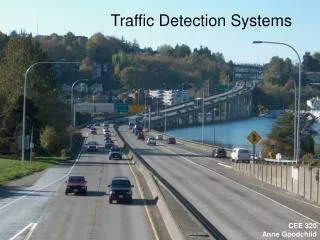

Detection systems
E N D
Presentation Transcript
Detection systems part 2
Electron microscope • electrons scatter when they pass through thin sections of a specimen • transmitted electrons (those that do not scatter) are used to produce image • denser regions in specimen, scatter more electrons and appear darker
Transmission electron microscope • Provides a view of the internal structure of a cell • Only very thin section of a specimen (about 100nm) can be studied • Magnification is 10000-100000X • Has a resolution 1000X better than light microscope • Resolution is about 0.5 nm • transmitted electrons (those that do not scatter) are used to produce image • denser regions in specimen, scatter more electrons and appear darker
Scanning electron microscope • No sectioning is required • Magnification is 100-10000X • Resolving power is about 20nm • produces a 3-dimensional image of specimen’s surface features • Uses electrons as the source of illumination, instead of light
Contrast formation Incident Electron Beam Contrast
Scanning probe microscopes • Characteristics of common techniques for imaging and measuring surface morphology from http://www.di.com/
Contact Mode AFM TappingMode™ AFM Non-contact Mode AFM Force Modulation Lateral Force Microscopy (LFM) Scanning Thermal Microscopy Magnetic Force Microscopy (MFM) LiftMode Phase Imaging Scanning Capacitance Microscopy Electric Force Microscopy (EFM) Nanoindenting/Scratching (IMHO) Scanning Tunneling Microscopy (STM) Lithography Scanning techniques
Scanning probe microscopes Type Properties used for scanning Resolution Used for STM Tunneling Current between sample and probe Vertical resolution < 1 Å *Lateral resolution ~ 10 Å => Conductors => Solids SP Surface profile Vertical resolution ~ 10 Å *Lateral resolution ~ 1000 Å • Conductors, insulators, semiconductors => solids AFM Force between probe tip and sample surface (Interatomic or electromagnetic force) Vertical resolution < 1 Å *Lateral resolution ~ 10 Å => Conductors, insulators, semiconductor => liquid layers, liquid crystals and solids surfaces MFM Magnetic force Vertical resolution ~ 1 Å *Lateral resolution ~ 10 Å => Magnetic materials SCM Capacitance developed in the presence of tip near sample surface Vertical resolution ~ 2 Å *Lateral resolution ~ 5000 Å => Conductors => Solids
Scanning probe microscopes • using scanning probe microscopes it is possible to image and manipulate matter on the nanometer scale • under ideal conditions its is possible to image and manipulate individuals atoms and molecules • this offers the prospect of important new insights in to the material world • this offers the prospect of important new products and processes
Scanning tunneling microscopes • using a scanning tunneling microscope it is possible to image individual nickel atoms
Scanning tunneling microscopes • it is also possible to manipulate individual iron atoms on a copper surface
Scanning tunneling microscopes • it is also possible to have some fun Iron on copper Carbon monoxide on platinum
Scanning tunneling microscopes • it is also possible to have some fun Xenon on nickel
Atomic force microscope • With an atomic force microscope it is possible to image the carbon atoms of a carbon tube.
Atomic force microscope • Or manipulate carbon tubes.
Atomic force microscope • Or have some fun again.
Scanning probe microscopes • thescanning tunnelling microscope (STM) is widely used to obtain atomically resolved images of metal and other conducting surfaces • this is very useful for characterizing surface roughness, observing surface defects, and determining the size and conformation of aggregates of atoms and molecules on a surface • increasingly STM is used to manipulate atoms and molecules on a surface • Roher and Binnig won the Nobel Prize in 1986 for their work in developing STM
Scanning probe microscopes • a conducting tip is held close to the surface • electrons tunnel between the tip and the surface, producing an electrical signal • the tip is extremely sharp, being formed by one single atom • it slowly scans across the surface at a distance of only an atom's diameter
Scanning probe microscopes • the tip is raised and lowered in order to keep the signal constant and maintain the distance • this enables it to follow even the smallest details of the surface it is scanning • by recording the vertical movement of the tip it is possible to study the structure of the surface atom by atom
Scanning probe microscopes • a profile of the surface is created • from that a computer-generated contour map of the surface is produced • limited to use with conducting substrates • this limitation was addressed by atomic force microscopy Logic gate
First atomic force microscope G. Binnig, Ch. Gerber and C.F. Quate, Phys. Rev. Lett. 56, 930 (1986)
Atomic force microscope • theatomic force microscope (AFM) is widely used to obtain atomically resolved images of non-metal and other non-conducting surfaces • this is very useful for characterizing chemical and biological samples • increasingly AFM is used to manipulate macromolecules and cells on a surface • Bennig, Quate and Geber are credited with developing AFM and have received many major awards
Atomic force microscope • an AFM works by scanning a ceramic tip over a surface • the tip is positioned at the end of a cantilever arm shaped like a diving board • the tip is repelled by or attracted to the surface and the cantilever arm deflected • the deflection is measured by a laser that reflects at an oblique angle from the very end of the cantilever
Atomic force microscope • Micofabricated cantilever beams and probe tips for AFM.