Update on IceMOS Wafer Shipment and Silicon Etching Results from GTK Collaboration Meeting
On December 3rd, important updates were shared at the GTK Collaboration meeting regarding the IceMOS project. The first wafers have been successfully shipped to CERN, with three bulk silicon wafers dispatched on December 10th. These wafers will be utilized to validate the final step of the fabrication process at EPFL, focusing on silicon etching with KOH to refine the cooling plate's acceptance area. Additionally, etching measurements from the initial nine bulk silicon wafers showed a channel etch depth of 70 µm ± 7 µm and a manifold etch depth of 285 µm ± 25 µm.

Update on IceMOS Wafer Shipment and Silicon Etching Results from GTK Collaboration Meeting
E N D
Presentation Transcript
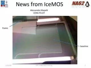
News from IceMOS Alessandro Mapelli CERN PH-DT frame baseline GTK Collaboration meeting
Schedule update December 3rd today Done.. First wafers sent to CERN GTK Collaboration meeting
Bulk Si vs SOI flows GTK Collaboration meeting
Silicon Etching • Etch measurements from the first 9 bulk silicon wafers Channels etch 70um +/- 7um Manifolds etch – total depth 285um +/- 25um IceMOS CONFIDENTIAL GTK Collaboration meeting
Silicon Etching IceMOS CONFIDENTIAL GTK Collaboration meeting
First wafers have been shipped.. • 3 bulk silicon wafers have been shipped on December 10th from IceMOS to CERN. • These wafers will be used to validate the last step of the fabrication process at EPFL with wafers from IceMOS. • It consists of the silicon etching with KOH to thin the acceptance area of the cooling plate. GTK Collaboration meeting