CSC 4250 Computer Architectures
230 likes | 390 Vues
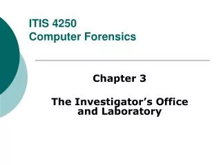
CSC 4250 Computer Architectures. December 1, 2006 Chapter 5. Memory Hierarchy. Figure 5.7. Data Cache in Alpha 21264. Data Cache Organization of Alpha 21264. The 64K cache is two-way set associative with 64-byte blocks The 9-bit index selects among 512 sets

CSC 4250 Computer Architectures
E N D
Presentation Transcript
CSC 4250Computer Architectures December 1, 2006 Chapter 5. Memory Hierarchy
Data Cache Organization of Alpha 21264 • The 64K cache is two-way set associative with 64-byte blocks • The 9-bit index selects among 512 sets • The circled numbers indicate the four steps of a read hit, in the order of occurrence • Three bits of the block offset join the index to supply the RAM address to select the proper 8 bytes. Thus, the cache holds two groups of 4096 64-bit words, with each group containing half of the 512 sets. • The line from lower-level memory is used on a miss to load the cache • The size of the address leaving the CPU is 44 bits because it is a physical address
Figure 5.8. Miss per 1000 instructions for instruction, data, and unified caches of different sizes. The percentage of instruction references is about 74%. The data are for 2-way associative caches with 64-byte blocks. (Is unified cache the worst choice?)
Cache Performance • Which has the lower miss rate: a 16KB instruction cache with a 16 KB data cache, or a 32 KB unified cache? • Use the miss rates in Figure 5.8 to help calculate the correct answer, assuming 36% of the instructions are data transfer instructions • Assume a hit takes 1 clock cycle and the miss penalty is 100 clock cycles • A load or store hit takes 1 extra clock cycle on a unified cache if there is only one cache port to satisfy two simultaneous requests (a structural hazard) • What is the average memory access time in each case? • Assume write-through caches with a write buffer, and ignore stalls due to the write buffer
Effective Miss Rates • Consider 16K instruction cache: Instruction miss rate = 3.82/1000 = 0.004 • Consider 16K data cache (36% of instructions are data transfers): Data miss rate = (40.9/1000)/0.36 = 0.114 • 74% of memory accesses are instruction references: Overall miss rate for split caches = (74%×0.004)+(26%×0.114) = 0.0324 • Consider 32KB unified cache: Miss rate = (43.3/1000)/(1.00+0.36) = 0.0318 • Thus, a 32KB unified cache has a slightly lower effective miss rate than two 16KB caches
Average Memory Access Time • Average Memory Access Time = % instructions × (hit time + instruction miss rate × miss penalty) + % data × (hit time + data miss rate × miss penalty) • Consider two 16KB split caches: Average Memory Access Time = 74%× (1 + 0.0038 × 100) + 26% × (1 + 0.1136 × 100) = 74%× 1.38 + 26% × 12.36 = 1.023 + 3.214 = 4.24 • Consider 32KB unified cache: Average Memory Access Time = 74%× (1 + 0.0318 × 100) + 26% × (1 + 1 + 0.0318 × 100) = 74%× 4.18 + 26% × 5.18 = 3.096 + 1.348 = 4.44 • The split caches, which offer two memory ports per clock cycle (thus avoiding the structural hazard), have a better average memory access time, despite having a worse effective miss rate
Cache Optimizations • Reducing miss penalty: multilevel caches, critical word first, read miss before write miss, merging write buffers, and victim caches • Reducing miss rate: larger block size, larger cache size, higher associativity, way prediction, and compiler optimization • Reducing miss penalty or miss rate via parallelism: hardware and compiler prefetching • Reducing time to hit in cache: small and simple caches, and pipelined cache access
Reducing Cache Miss Penalty • Multilevel Caches • Critical Word First and Early Restart • Giving Priority to Read Misses over Writes • Merging Write Buffer • Victim Caches
1. Multilevel Caches • Performance gap between processors and memory leads to the question: Should one make the cache fast enough to keep pace with the speed of the CPUs, or make the cache large enough to overcome the widening gap between the CPU and main memory?
Answer • Both • Add another level of cache between the original cache and memory. The first-level cache is small enough to match the clock cycle time of the fast CPU, and the second-level cache is large enough to capture many accesses that would otherwise go to main memory.
Two-Level Cache System • Local miss rate ─ the number of misses in a cache divided by the total number of memory accesses to this cache • Global miss rate ─ the number of misses in the cache divided by the total number of memory accesses generated by the CPU. Thus, the global miss rate for the first-level cache is just its local miss rate, but the global miss rate for the second-level cache is the product of the local miss rates of the first and second level caches.
Example • Suppose that in 1000 memory references there are 40 misses in the first-level cache and 20 misses in the second-level miss. What are the various miss rates? • Assume the miss penalty from L2 cache to memory is 100 clock cycles, the hit time of L2 cache is 10 clock cycles, the hit time of L1 cache is 1 clock cycle, and there are 1.5 memory references per instruction. What is the average memory access time?
Answer • The miss rate (either local or global) of the first-level cache is 40/1000 or 4% • The local miss rate for the second-level cache is 20/40 or 50% • The global miss rate of the second-level cache is 20/1000 or 2% • Average memory access time = 1 + 4% × ( 10 + 50%×100 ) = 3.4 clock cycles
Multilevel Inclusion • Multilevel inclusion is natural for memory hierarchy: L1 data are always present in L2. Inclusion is desirable because consistency between I/O and caches can be determined by just checking the second-level cache. • Many cache designers keep the block size same in all levels of caches • What if the designer can afford only an L2 cache that is slightly larger than the L1 cache? • An example is the AMD Athlon: two 64KB L1 caches and only one 256KB L2 cache • Should a significant portion (50% in Athlon) of the L2 space be used as a redundant copy of the L1 cache?
Multilevel Exclusion • Athlon: L1 data is never found in an L2 cache • With this policy, a cache miss in L1 (followed by a cache hit in L2) results in a swap of blocks between L1 and L2 instead of a replacement of an L1 block with an L2 block
2. Critical Word First and Early Restart • Critical word first ─ Request the missed word first from memory and send it to the CPU as soon as it arrives; let the CPU continue execution while filling the rest of the words in the block • Early restart ─ Fetch the words in normal order, but as soon as the requested word of the block arrives, send it to the CPU and let the CPU continue execution
3. Giving Priority to Read Misses over Writes • Serve reads before writes are completed • What about write buffers? They might hold the updated value of a location needed on a read miss. • Example SW R3,512(R0) ;M[512]←R3 (cache index 0) LW R1,1024(R0) ;R1←M[1024] (cache index 0) LW R2,512(R0) ;R2←M[512] (cache index 0) • Assume a direct-mapped, write through cache that maps 512 and 1024 to the same block, and a four-word write buffer • Will the value in R2 always be equal to the value in R3? • What is the data hazard in memory? • RAW
RAW Hazard in Memory • The data in R3 are placed into the write buffer after the store. The first load uses the same cache index and is therefore a miss. The second load tries to put the value in location 512 into R2; this also results in a miss. If the write buffer has not completed writing to location 512 in memory, the read of location 512 will put the old, wrong value into the cache block, and then into R2. • Without proper precaution, R3 would not equal R2!
Solution • One way is to require the read miss to wait until the write buffer is empty • An alternative is to check the contents of the write buffer on a read miss
Cost of Writes in Write-back Cache • How to reduce the cost of writes in a write-back cache? • Suppose a read miss replaces a dirty cache block. Instead of writing the dirty block to memory, and then reading memory, we could copy the dirty block to a buffer, then read memory, and finally write memory. Now the CPU read will finish sooner. If a read miss occurs, the processor should either stall until the buffer is empty or check the addresses of the words in the buffer for conflicts (same as above for write-through).
4. Merging Write Buffer • Without write merging, the words to the right in the upper part of the figure would only be used for instructions that write multiple words at the same time • This optimization reduces stalls due to the write buffer being full
5. Victim Caches • Victim cache: small, fully associative • AMD Athlon: victim cache with eight entries • Although it reduces the miss penalty, the victim cache is aimed at reducing the damage done by conflict misses