Download
1 / 1
20 likes | 349 Vues
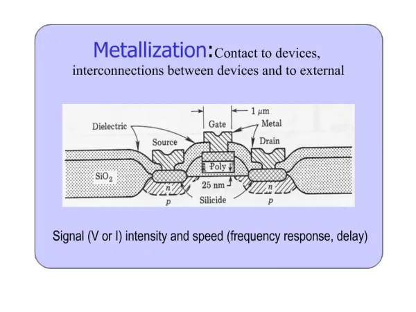
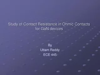
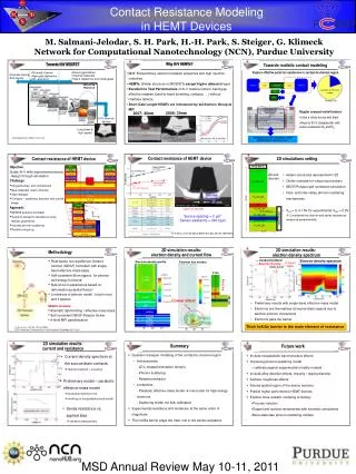
Contact Resistance Modeling in HEMT Devices. Virtual Source. E F. 0 nm. E F. 2D sim. domain. E F. E F. In 53 Ga 47 As. Plot Line. M. Salmani-Jelodar, S. H. Park, H.-H. Park, S. Steiger, G. Klimeck Network for Computational Nanotechnology (NCN), Purdue University. In 52 Al 48 As.

E N D
Contact Resistance Modeling in HEMT Devices Virtual Source EF 0 nm EF 2D sim. domain EF EF In53Ga47As Plot Line M. Salmani-Jelodar, S. H. Park, H.-H. Park, S. Steiger, G. Klimeck Network for Computational Nanotechnology (NCN), Purdue University In52Al48As region of interest 90nm 100 nm InP In52Al48As EF Si δ-doping EF In53Ga47As InAs virtual drain In53Ga47As Why III-V HEMTs? Towards III-V MOSFET Towards realistic contact modeling In52Al48As Explore effective parts for resistances in contact-to-channel region. • Device geometries • Channel materials • High-k dielectrics and metal gates • III-V: Extraordinary electron transport properties and high injection velocities • HEMTs: Similar structure to MOSFETs except high-κ dielectric layer • Excellent to Test Performances of III-V material (strain, band gap, effective masses, band-to-band tunneling, contacts, …) without interface defects • Short Gate Length HEMTs are Introduced by del Alamo’s Group at MIT • Strained channel • New gate dielectrics: • HfO2 and Al2O3 40nm • Channel doping • S/D doping Channel region Contact 1 Contact 2 2015-2019 Research Lead 1 channel Lead 2 Contact-to-channel region channel channel Device Pie • Regular compact model features: • Uses a virtual source and drain. • Need to fit I-V characteristic with series resistances RS and RD. Simulation Domain 2008: 30nm 2007: 40nm III-V channel devices Low-power & high-speed Acknowledgement: Robert Chau, Intel Simulation domain of compact model (IEDM 2009, N. Kharche et al.) D.H. Kim et al., EDL 29, 830 (2008) Contact resistance of HEMT device 2D simulations setting Contact resistance of HEMT device • Objective: Guide III-V InAs experimental device design through simulation • Challenge: • 2D geometries, and confinement • New materials, strain, disorder • Gate leakage • Contacts – scattering, disorder, and curved shape. • Approach: • NEMO5 quantum simulator • Quantum transport simulations using realistic geometries • Includes phonon scattering • Parallel computing Source Drain N+ Cap In0.53Ga0.47As N+ Cap In0.53Ga0.47As 25nm • Hetero-structures represented in 2D • Ohmic contacts for virtual source/drain • NEGF/Poisson self-consistent simulation • Intra- and inter-valley phonon scattering mechanisms • VDS = 0~0.15V for experimental VDD = 0.5V • Considered the channel and series resistances measured experimentally In0.52Al0.48As In0.52Al0.48As InP InP Gate In0.52Al0.48As In0.52Al0.48As In0.52Al0.48As In0.53Ga0.47As InAs In0.53Ga0.47As In0.52Al0.48As Contact Pad Rpad N+ Cap InGaAs 35nm Rcap In0.52Al0.48As 15 nm Y Source spacing = 2 μm* Series resistance = 240 Ωμm InP etch stop 6 nm In0.52Al0.48As X Rbarrier 11 nm 2 nm In0.53Ga0.47As Rside InAs 5 nm Virtual Drain 3 nm In0.53Ga0.47As In0.52Al0.48As *D.-H. Kim, J. D. A. del Alamo, IEEE Trans. Elec. Dev. 57, 1504 (2010) 500nm 2D simulation results: electron density and current flow 2D simulation results: electron density spectrum Methodology --- Conduction Band --- Electron Density • Real-space non-equilibrium Green’s function (NEGF) formalism with single-band effective-mass basis • Self-consistent Born approx. for phonon self-energy functions1 • Bulk phonon parameters based on deformation potential theory2 • Limitations of phonon model : local in real and k spaces Electron density spectrum Electron density profile Electron flux vectors δ-doped Layer InAlAs barrier n+ cap InGaAs (/cm3) (a.u.) n+ cap channel InAlAs Corner effect InP • Preliminary results with single-band effective-mass model • Electrons are thermalized at source/drain regions due to electron-phonon interactions • Electrons pass the barrier 0 • NEMO5 simulator: • Atomistic tight-binding / effective-mass basis • Self-consistent NEGF-Poisson Solver • 4-level MPI parallelization InAlAs InGaAs InAs InGaAs InAlAs Thick InAlAs barrier is the main element of resistance [1] S. Jin et al., JAP 99, 123719 (2006) [2] M. Lundstrom, Fundamentals of carrier transport (Cambridge Univ. Press) 2D simulation results: current and resistance Summary Future work • Quantum transport modeling of the contact-to-channel region • Achievements: - 2D L-shaped simulation domain • - Phonon scattering • - Resistive behavior • Limitations: - Parabolic effective-mass model inaccurate for high energy electrons • - Scattering model not fully calibrated • Experimental resistance and model are at the same order of magnitude • The InAlAs barrier plays the main role in the series resistance • Include nonparabolic band structure effects • Improving phonon scattering model • – calibrate against experimental mobility models • Include alloy disorder effects, impurity / doping disorder • Surface roughness effects • Extend spatial region of the device sections • Predict higher performance HEMT devices • Explore more realistic modeling including: • Process variation • Dopant and surface randomness with atomistic simulations • More elaborate phonon scattering models • Current density spectrum at the source/drain contacts • thermal injection + tunneling • Preliminary model – parabolic effective-mass model • conduction band too low • working on nonparabolic band model • Series resistance vs. applied bias • resistive characteristic