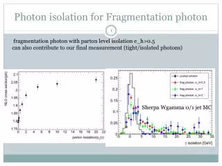
Photon detection
Photon detection. Visible or near-visible wavelengths Need photosensitive element and transparency (long λ abs length ) Generate photoelectron (or e-h pair), amplify and collect signal Photomultiplier tubes Workhorse; sensitive, relatively cheap, operating issues Si photodiodes

Photon detection
E N D
Presentation Transcript
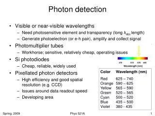
Photon detection • Visible or near-visible wavelengths • Need photosensitive element and transparency (long λabs length) • Generate photoelectron (or e-h pair), amplify and collect signal • Photomultiplier tubes • Workhorse; sensitive, relatively cheap, operating issues • Si photodiodes • Cheap, reliable, widely used • Pixellated photon detectors • High efficiency and good spatialresolution (e.g. CCD) • Issues around data readout speed • Developing area Color Wavelength (nm) Red 625 – 740Orange 590 – 625Yellow 565 – 590Green 520 – 565Cyan 500 – 520Blue 435 – 500Violet 380 - 435 Phys 521A
Photodetector device characteristics • Quantum efficiency (photoelectrons/incident photon) • Collection efficiency (geometrical acceptance, etc) • Gain: electrons collected per photoelectron • Dark current: signal in absence of light (noise) • Energy resolution: function of signal statistics and noise level • Dynamic range: difference between single photon and input optical power at which signal saturates • Time response: delay and width of electrical signal relative to incident photon time • Rate capability: How quickly can subsequent photons be registered? Phys 521A
Photomultiplier tubes • Evacuated tube supplied with high voltage (many 100s of volts) • Photocathode ejects electrons (PE effect) • E-field accelerates them toward surface (dynode) with low work function, liberating additional electrons • Amplification factor of 3-5 per dynode; many stages lead to large 104-107 amplification factors (resistive voltage divider network) that can be tuned via operating voltage • Cannot operate in strong B fields (ev x B force) • Dark current (leakagecurrent, thermionicand field emission);fn of operating voltage • Need special windowsfor input in UV Phys 521A
More on PMTs • Light collection area can be large (50cm diameter in Super-K) • Spectral response (photocathode): Lake Super-K Phys 521A
Large range of PMT choice • Hamamatsu tubes (part of catalog of >400 models) Phys 521A
Silicon Photodiodes • P-N junction; input photon creates e-h pair, pushing e into conduction band • P-layer collects holes, N-layer collects electrons • Features: • High quantum efficiency • Linear flux response • Spectral response peaked toward “red” • Insensitive to B fields • Low noise (dark current) Phys 521A
Photodiode Specifications • Hamamatsu specs (of ~80) • Absorption strong fn of wavelength Phys 521A
Avalanche Photodiodes • Photodiodes with large reverse bias (>100 V) applied • Large bias accelerates liberated electrons, causing them to create additional e-h pairs (avalanche) • Signal amplification is strong function of bias • for moderate bias the signal remains proportional to the input, but bias and temperature must be controlled • Large bias generates large, saturated signal (“Geiger”mode, output signal independent of input signal size) • Large quantum efficiencies possible, along with sub-ns time response Phys 521A
PMT/APD comparison • PMT and avalanche-photodiode response must be matched to the output spectrum from the scintillator used; some common examples shown here Phys 521A
Pixellated photon detectors (PPD) • Recent development – solid state devices based on arrays of avalanche photodiodes • Also known as “SiPM, or silicon photomultipliers” • Create large array (~103 APDs) packed into small (~1mm2) area • Each APD operates in limited Geiger mode (binary signal) • Count photons by digitally summing cell outputs • Goal is to obtain CCD-like efficiency and spatial resolution with fast, integrated readout (combined manufacture of PPD and ASIC) ASIC = application specific integrated circuit, i.e. custom electronic chip Phys 521A
PPD used by T2K • Hamamatsu MPPC – array of APD operated in Geiger mode • 50x50μm pixels; 667/device • Operating voltage ~70V; quantum efficiency ~15% @ 550nm Phys 521A
Scintillators Phys 521A
Scintillation counters • Workhorse of particle detectors • Ionization from charged particles excites molecules; de-excitation results in scintillation light • Two main types: organic (e.g., hydrocarbons) and inorganic (crystals, like NaI) • Important co-process is fluorescence, where photon excites a molecule (fluor) which subsequently de-excites via a longer wavelength photon • Fluors are needed both to avoid self-absorption and to enable better spectral match to photon detectors • Only few % of deposited energy converted to scintillation light Phys 521A