Download
1 / 10
100 likes | 252 Vues
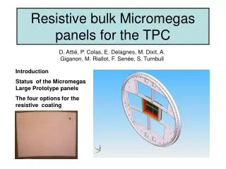
Micromegas chamber 1m² design. W based HCAL prototype meeting 2010, March 2nd. 1m² Micromegas chamber. External frame. Top plate (made of W). 6 ASU. Vetronit mask (holes machined for electronic devices to be inserted). Electronic boards. Bottom plate (made of W).

E N D
Micromegas chamber 1m² design W based HCAL prototype meeting 2010, March 2nd
1m² Micromegas chamber External frame Top plate (made of W) 6 ASU Vetronit mask (holes machined for electronic devices to be inserted) Electronic boards Bottom plate (made of W)
External dimensions – option 1 1160 mm OPTION 1: Large plates with holes 999 mm Electronic boards (inter_DIF & DIF) 1024 mm
External dimensions – option 1 OPTION 1: Large plates with holes Space and holes to hang the chamber (rail)
External dimensions – option 2 OPTION 2: Smaller plates 1160 mm 999 mm 1004 mm 1024 mm
External dimensions – option 2 OPTION 2: Smaller plates • Reduce the plates size • reduce the volume without detection • get the active area as close as possible to the chamber overall dimensions Insertion of the chamber like a cassette
1m² Micromegas chamber 26.8 mm 965.6 mm 16.7 mm ACTIVE AREA = 965.6mm x 970.4 mm 970.4 mm 16.7 mm Picture with option 1 plates ( BUT the active area remains unchanged for option 2 ) 26.8 mm
1m² Micromegas chamber Top plate removed 6 ASU (pads side)
1m² Micromegas chamber [ Chamber cross section ] PCB + bulk (1.5 mm) W plate (2mm) + copper foil (5 μm) Internal spacer 5mm 3 mm drift gap Machined mask (3mm) W plate (2mm) 2mm Chamber total thickness = 2 + 3 + 1.5 + 3 + 2 = 11.5 mm
1m² Micromegas chamber Dimensions of the electronic boards DIF (1.5mm thick) Inter_DIF (1.6mm thick) 130 mm 999 mm 13.5 mm 1160 mm 11.5 mm 9 mm 3 mm 5 mm