Bulk Micromegas
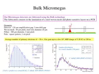
Bulk Micromegas. Our Micromegas detectors are fabricated using the Bulk technology The fabrication consists in the lamination of a steel woven mesh and photo-sensitive layers on a PCB. Geometry Detector : 128 μm amplification gap, 3 mm drift gap

Bulk Micromegas
E N D
Presentation Transcript
Bulk Micromegas Our Micromegas detectors are fabricated using the Bulk technology The fabrication consists in the lamination of a steel woven mesh and photo-sensitive layers on a PCB Geometry Detector : 128 μm amplification gap, 3 mm drift gap Woven mesh : 80 μm pitch, steel wire diameter 20 μm Pillars : 300 μm diameter, 2 mm pitch Pads : square pattern, 1 cm pitch Average number of primary electrons of ~ 30 e-, Gas gain up to a few 104, MIP charge of 5-20 fC in 150 ns Landau distribution in a small chamber (96 pads) C. Adloff, 2009 JINST 4 P11023 2 GeV e- profile in a virtual ECAL, C. Adloff 2010 JINST 5 P01013
Micromegas boards (ASU) The basic building block of our large area Micromegas chamber is an 8 layer PCB of 32x48 cm2 It is equipped with 24 ASICs, 1536 pads and a Bulk mesh It is called an Active Sensor Unit (ASU) ASU can be chained thanks to flexible inter-connections They are also equipped with spark protections (diodes) They are read out by 2 boards: DIF & interDIF (cf. photograph) 32x48 pads of 1 cm2 on mesh side 24 ASIC + spark protections on back side Power, digital signals, calibration, PC link Spark protections ASIC Flex. interconnects Flex. Interconnects to next ASU Mesh HV
The MICROROC is a 64 channel chip developed with LAL/Omega 3 discriminators Second level of spark protection Memory & timestamp Low noise preamp. (3000 ENC) Shapers (75-200 ns) Front-end electronics Following the ILC beam time structure, the front-end electronics: - is off between bunch trains → power-pulsing of analogue part; - is on during trains → self-triggering capability + memory with 200 ns timestamping; It is well suited for both Micromegas and GEMs → Will be used with THGEM during Nov. test beam
trigger efficiency trigger efficiency ASU characterisation Electronics calibration: align pedestals to reduce threshold dispersion to ~ 1 fC 1 ASIC 1 ASIC 1 ASU (24 ASIC) Operation inside a gas chamber: 55Fe quanta peaks aboveflat (cosmic) background: no noise!
Design of the 1 m2 chamber The 1 m2 chamber consists of 3 slabs with DIF + interDIF + ASU + ASU This design introduces very little dead zone (below 2%) and is fully scalable to larger sizes The drift gap is defined by small spacers and a frame The final chamber thickness is 9 mm Drift cover Frame with 2 gas pipes ASU (mesh) Spacers Readout boards (DIF+interDIF) Also provide ASIC LV & mesh HV
Efficiency and multiplicity – 2 prototypes inside SDHCAL 287 ASIC Performance to MIPs A high efficiency to MIPs is reached at a gas gain of 3000 (390 V) Due to the small spread of charge in the Micromegas, the hit multiplicity is between 1.1-1.2 at 90° incidence Efficiency & multiplicity VS mesh HV (Standalone test) The efficiency variation over 287 ASIC (8x8 cm2 regions) is 2% RMS, for an average of 96% → Very good control of the chamber dimension and thresholds
Performance to hadrons Hadron showers contain heavily ionising particles (& a few MIPs) → what is the necessary gas gain? From the distribution of the number of hits at various voltages... probably less than 1000! Indeed, the tails of the distributions at 350 V and 375 V are very similar. XY occupancy & number of hits Exp. setup traversing pions showering pions 1 m2 chb. 1 λint of Fe 150 GeV π
About 500 thousands channels in 1 m3 . Pions simultaneously showering in the SDHCAL Colors stand for the 3 thresholds Performance inside CALICE/SDHCAL The SDHCAL is a 50 layers sampling calorimeter (~ 6 λint) of steel absorbers and 1 m2 active layers During a test beam in May, the SDHCAL was equipped with 48 RPCs and 2 Micromegas All detectors were all read out by a common DAQ
100 Gev pions layer 49/50 100 Gev muons layer 49/50 med. thr ~ 1 MIP high. thr ~ 5 MIP low thr ~ 1 fC Performance inside CALICE/SDHCAL The distributions measured in the Micromegas chambers are well reproduced by MC simulation Average Nhit versus pion energy No saturation at the back of SDHCAL → linear response of 3 thresholds
Future plans Shower profiles with 3 Micromegas chambers Novembre 2012 test beam inside SDHCAL 46 RPCs and 4 Micromegas at layers 10-20-35-50 Identify shower start z0 with RPCs and measure Nhit in Micromegas chambers w.r.t. z0 In this way the shower longitudinal profile w.r.t. z0 can be obtained Integration of the profiles at various energies yields the response of a full Micromegas SDHCAL! Simulation R&D in 2013: Spark Protection in Large Area Micromegas project (SPLAM) Reduce PCB cost by replacing the passive spark protections by a resistive layer on the anode surface We did some simulation and will fabricate and test prototypes Simulation of the maximum voltage drop on the pads during a spark