Download
1 / 19
200 likes | 364 Vues
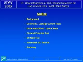
Background Continuity / Leakage Current Tests Diode Breakdown / Opens Tests Channel Potential Test DC Gain Test Automated DC Test Set Summary. Outline. Background :.

E N D
Background • Continuity / Leakage Current Tests • Diode Breakdown / Opens Tests • Channel Potential Test • DC Gain Test • Automated DC Test Set • Summary Outline Ball Aerospace & Technologies Corp.
Background: • Problem: How to quickly and accurately qualify scientific grade CCDs prior to integration into complex packages and/or multi-chip focal plane arrays (e.g. HiRISE and NPOESS-OMPS )? • Full functional (a.k.a. EO or AC) characterization of incoming CCD detectors can sometimes only be performed after expensive package assembly steps have been completed • Discovering CCD tolerance issues after complex packaging steps is expensive and can significantly impact development schedules • EO testing alone does not adequately reveal all potential problems • For example, if Yth and/or Vin for one clock phase significantly differs from the other clocks or inadequate tolerance range • Performing thorough DC characterization is an effective way to quickly and accurately qualify CCDs HiRISE Multi-Detector FPA NPOESS-OMPS FPA Ball Aerospace & Technologies Corp.
Background: • The DC tests of most interest in detector screening are: • Continuity Yields pin-to-pin resistance, verifies process, checks for gross ESD damage, and verifies detector arrived without damage • Leakage Current Yields static current draw on each gate, checks for subtle ESD damage, and verifies detector arrived without latent damage • Diode Breakdown Verifies process, and confirms adequate operating margins on drain biases (e.g. OD, RD, and ID) • Diode / Opens Checks for open circuits (e.g. bad/missing wirebonds), verifies diode operation, and checks for intra-layer continuity (e.g. poly 1 to poly 1) • Channel Potential Yields threshold potential and inversion voltage for each gate, verifies optimal clock and bias operating points, and confirms tolerance ranges • DC Gain Verifies amplifier operating point and voltage tolerance ranges • A brief introduction to each of these measurements will be presented followed by some examples of the usefulness of measurements Ball Aerospace & Technologies Corp.
Continuity & Leakage Current Tests: • Continuity Test • Group two sets of pins together and force a small current (e.g. 1 uA) between the two sets • To protect CCD detector, the voltage compliance (i.e. the maximum voltage allowed to develop across the two sets of pins) is set to a relatively low voltage, for example +15 volts • If the resistance between the sets of pins is high, voltage compliance will be reached and the test will pass. • If voltage compliance is not reached, the test is failed and the resultant voltage (and resistance) is reported. • All combinations of gate-to-gate and gate-to-substrate continuity measurements should be performed on every CCD (e.g. OG vs. Sub & R1 vs. R2, etc.) I Continuity Measurement Setup + I 1 V 2 - Continuity Test Equivalent Circuit Ball Aerospace & Technologies Corp.
Continuity & Leakage Current Tests: • Leakage Current Test • Group two sets of pins together and force a small voltage (e.g. +15 v) between the two sets • To protect CCD detector, the current compliance (i.e. the maximum current allowed to flow between the two sets of pins) is set to a relatively low level, for example 1 uA • If current compliance is not reached and the resultant current is below specification, then the test is passed and the resultant current is reported. • If the resistance between the sets of pins is low, current compliance will be reached and the test will fail. • All combinations of gate-to-gate and gate-to-substrate leakage current measurements should be performed on every CCD (e.g. OG vs. Sub & R1 vs. R2, etc.) Leakage Current Measurement Setup + 1 I V - 2 Leakage Current Test Equivalent Circuit Ball Aerospace & Technologies Corp.
Diode Breakdown & Diode Opens Tests: • Diode Breakdown Test • Sweep reverse bias on a diode input vs. substrate from 0 to absolute maximum value specified by CCD vendor • To protect CCD detector, the current compliance (i.e. the maximum current allowed to flow in the diode) is set to a relatively low level, for example 5 to 10 uA - value dependent on area of diode • If current compliance is not reached or it is reached and the corresponding voltage meets specification, then the test passes • If current compliance is reached and the corresponding voltage does not meet specification, then the test fails • All input diode pins should be tested vs. substrate (e.g. OD, OS, RD, and ID) • As a precaution this test should not be performed on flight candidate CCD detectors Diode Breakdown Measurement Setup + 1 I V - 2 Diode Breakdown Test Equivalent Circuit Ball Aerospace & Technologies Corp.
Diode Breakdown & Diode / Opens Tests: • Diode / Opens Test • Apply a fixed forward bias voltage (e.g. 2 v) between a diode input and substrate or between two redundant input signals • To protect CCD detector, the current compliance (i.e. the maximum current allowed to flow in the diode) is set to a relatively low level, for example 10 to 50 uA • If current compliance is reached, then the conduction path has a low impedance and the test passes • If current compliance is not reached, then the impedance path is high and the test fails • This test should be performed on all diode vs. substrate combinations and between all redundant signals (e.g. R01A vs. R01B) Diode / Opens Measurement Setup + 1 V I - 2 Diode / Opens Test Equivalent Circuit Ball Aerospace & Technologies Corp.
Channel Potential Test: • Channel Potential (CP) testing yields the threshold potential (Yth) and inversion voltage (Vin) under many, sometimes all, gates on a CCD detector • These two parameters are key for establishing clock and bias operating levels and tolerances • The basic CP measurement requires a gate surrounded by two drains • One drain is statically biased on (“Source” in figure) • A small current is sourced into the other drain (“Drain” in figure), which electrically “floats” to the potential under the controlling gate • Voltage on gate of interest is swept and the “Drain” voltage (i.e. the gate channel potential) is measured • Channel potential testing yields the most information on CCDs with 3 or 4 F architectures, but CCDs with 2 F architectures can also yield significant data • Channel Potential (CP) testing can be performed to some extent on almost all CCD detectors • Most CCD vendors monitor CP test structures on wafers but significant differences from actual CCD data can exist Basic channel potential measurement on a MOSFET Typical channel potential curve Ball Aerospace & Technologies Corp.
(a) (b) (c) (d) Channel Potential Test: • Determining the best measurement path requires complete design information, which vendors are usually willing to provide • Split readout serial registers (see (b)), single readout serial registers with electrical injection (see (c)), and parallel registers with electrical injection are ideal architectures for CP measurements on CCD • Since access to the internal circuitry is quite limited in CMOS based detectors CP measurements are generally not possible Common measurement paths for channel potential testing Ball Aerospace & Technologies Corp.
Channel Potential Test: • All gates in between the measurement drains, other than the gate being measured, must be turned “on” so they don’t influence results • Other measurement paths must be removed by turning “off” some gates • e.g. If measuring SWA and using two RD drains on either side of the serial register, the parallel register clocks need to be “off” • Typical measurement current is 20 nA • To high a value can induce a significant I.R voltage drop Channel potential setup for Summing Well A (SWA) gate using two amplifier RD drains Ball Aerospace & Technologies Corp.
Channel Potential Test: • Using CP data and design tolerances, complete CP diagrams for the entire CCD can be easily generated • Example here uses +/- 0.1 v design tolerance • Accurately quantifying changes in Yth as a function of radiation exposure level is needed for space-based applications Note the significant shift in serial phase 2 (R2) CP from other serial phases Ball Aerospace & Technologies Corp.
DC Gain Test: • Test measures the small signal gain of each on-chip amplifier by sweeping the reset drain voltage (with reset gate on) and measuring the resultant DC output voltage • Output MOSFET is biased using a constant current load of typically 2 mA • Small signal gain is calculated using • Typical DC gain values range between 0.5 and 0.8 depending on the amplifier configuration (e.g. 1, 2, or 3 stages) • DC gain or equivalent measurements are generally not possible on CMOS based detectors since access to the internal circuitry is limited DC Gain Measurement Setup DC gain test equivalent circuit Ball Aerospace & Technologies Corp.
DC Gain Test: • Any type of CCD charge-to-voltage amplifier can be measured (e.g. single stage, dual stage, and AC coupled stage) • Optimal operating point and adequate bias tolerances can be quickly verified (both pre and post radiation) • “Bad” MOSFETs can be quickly identified Common CCD Output Amplifier Configurations: (a) Single-Stage Source Follower, (b) Two-Stage Source Follower, (c) Two-Stage Source Follower with Bias Control, and (d) AC Coupled, Two-Stage Source Follower Ball Aerospace & Technologies Corp.
DC Gain Test: • A typical input (RD) versus output (OS) curve is shown at right along with small signal gain • Slope of small signal gain curve around operating point gives a measure of the low frequency linearity response Direction of Increasing Signal Output Response and Small Signal Gain for a typical DC coupled amplifier • AC coupled amplifiers yield a slightly different shaped DC gain curve due to the presents of the line reset MOSFET • Two distinct cutoff points are observed • Line reset MOSFET cut off point • Reset MOSFET cut off point • Gate of line reset MOSFET should be held “off” during the entire scan Example of DC gain curve for AC coupled two stage amplifier Ball Aerospace & Technologies Corp.
Computer Matrix HP4141 DC Adapter Box Automated DC Test Set: • Basic components of a fully automated DC test set are • A programmable cross point matrix to make/break all required connections • A programmable DC Parameter Analyzer • At least 4 Stimulus/Measurement Units (SMUs) are needed, but having more than 4 enables other DC measurements • Generic DC adapter box (supports automated and manual DC testing) • Personal Computer with GPIB (IEEE-488) interface • Single DC adapter board per detector • All DC measurements described here can also be performed manually using accurate current / voltage sources and meters • Very time consuming! Automated DC test set at Ball Aerospace & Technologies Corp Each detector requires only a simple DC adapter board, all other hardware is common Ball Aerospace & Technologies Corp.
Automated DC Test Set: • All test equipment is controlled through a single, simple program • User friendly GUI allows wide range of user (operator engineers) • Priority access prevents operators from making changes to critical parameters • All test results and conditions are stored automatically after each test • Interactive measurements possible using HP4141 virtual instrument interface • Test results easily imported to other analysis programs (e.g. Excel, IDL) Automated DC test set interface software – Channel potential test example shown Ball Aerospace & Technologies Corp.
Summary: • Some examples of problems identified during DC testing • ESD damage occurring during packaging/shipping • Processing problems (e.g. low diode breakdowns) • Non-optimal amplifier operating point • Non-optimal bias levels (e.g. OG, RD or OD) • Inadequate bias tolerances • To account for variability in electronics design, within CCD population, or resulting from post radiation shifts Example of bad recommended DC operating point Non-Optimal OD Operating Point Range Example of bad recommended OD bias point Example of gate to gate channel potential variability Ball Aerospace & Technologies Corp.
Summary: • DC characterization provides a fast, accurate, and thorough means for evaluating incoming CCD detectors • Thorough DC characterization does not replace full AC characterization but does significantly speed the process of AC characterization and FPA build up • It allows the build up of complex and expensive multi-detector FPAs to proceed with high confidence that all CCDs are “healthy” and have necessary clock and bias tolerances • Thorough DC characterization on CCDs early on in a program can identify processing and design problems • Most CCD vendors do not perform such exhaustive DC testing on CCDs (wafer level or packaged) due to time/cost • DC testing during pre/post radiation studies is recommend • Thorough DC and AC characterization enables fixed voltage systems to be employed in space-based applications with high confidence • DC characterization provides vital information for pre/post radiation testing (e.g. see examples ) DC data from pre/post radiation and vac-bake experiments Ball Aerospace & Technologies Corp.
Summary: • Complete DC testing is performed on all incoming CCDs at Ball, often multiple times during assembly of a FPA • Recommended order for performing DC tests is shown in tables at right • A subset of the DC tests presented can also be performed on CMOS based detectors • Due to intervening circuitry, however, it is usually not possible to perform the channel potential and DC gain tests • Questions? • Contact information: Rob Philbrick Ball Aerospace & Technologies Corp. P.O. Box 1062, Mail Stop: CO-5 Boulder, CO 80306 (303) 939-5399 rphilbri@ball.com Recommended Order for DC Testing CCD CMOS * As a precaution, the diode breakdown testing should not be performed on flight candidate detectors Ball Aerospace & Technologies Corp.