Download
1 / 27
430 likes | 1.17k Vues
Sensors Interfacing. Sensors to ADC. Sensors Output span rarely fit input span of ADC Offset (a) – require level shifting Unequal span (b) – require amplification Both (c) –Require both level shift and amplification An OpAmp Level shift and amplify simultaneously. Interfacing components.

E N D
Sensors to ADC • Sensors Output span rarely fit input span of ADC • Offset (a) – require level shifting • Unequal span (b) – require amplification • Both (c) –Require both level shift and amplification • An OpAmp Level shift and amplify simultaneously
Interfacing components • OPAMP • Filters • Comparators • ADC • Voltage References
Op-amp Characteristics • High Input resistance • Low Output resistance • Ability to drive capacitive load • Low input offset voltage • Low input bias current • Very high open loop gain • High common mode rejection ratio
OPAMP classification criteria • Precision opamp • Single/dual supply opamp • Single ended/differential opamp • High Bandwidth opamp • Rail to rail IO opamp
Unity gain – Voltage follower • Provide impedance conversion from high level to low level • A follower design should have following characteristics • For current generating sensors – input bias current of opamp should be at least hundred time smaller than sensors current • Input offset voltage should be smaller than required LSB
Instrumentation Amplifier • Three opamp IA configuration • A IA amplifies the difference between V+ and V-
Instrumentation Amplifiers • IA are available as monolithic IC’s • Fixed gain range • Easy to set desired gain using a single resistor • Very high CMRR of the order of 100db and more
Filters • To remove unwanted signal components in the input signal • Analog Filters • Passive filters • Designed using passive R,L,C components • Simple to design 1st order filters • Active filters • Based on active component like transistors or opamp • Possible to amplify signal of interest • Digital Filters
High-pass response Low-pass response Categories of Filters Low Pass Filters: pass all frequencies from dc up to the upper cutoff frequency. High Pass Filters: pass all frequencies that are above its lower cutoff frequency
Band Pass Response Band Stop Response Categories of Filters Band Pass Filters: pass only the frequencies that fall between its values of the lower and upper cutoff frequencies. Band Stop (Notch) Filters: eliminate all signals within the stop band while passing all frequencies outside this band.
Single-Pole Low/High-Pass Filter High Pass Filter Low Pass Filter
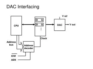
DAC • Is a circuit whose output depend on digital input and associated reference voltage • DAC can be implemented using PWM • for PWM • Vavg=(Ton/T) X Vlh • PWM output filtered using RC filter
ADC Essentials • Basic I/O Relationship • ADC is Rationing System • x = Analog input / Reference • Fraction: 0 ~ 1 n bits ADC Number of discrete output level : 2n Quantum LSB size Q = LSB = FS / 2n Quantization Error 1/2 LSB Reduced by increasing n
Conversion PARAMETERS • Conversion Time • Required time (tc) before the converter can provide valid output data • Input voltage change during the conversion process introduces an undesirable uncertainty • Full conversion accuracy is realized only if this uncertainty is kept low below the converter’s resolution • Converter Resolution • The smallest change required in the analog input of an ADC to change its output code by one level • Converter Accuracy • The difference between the actual input voltage and the full-scale weighted equivalent of the binary output code • Maximum sum of all converter errors including quantization error
Converting bipolar to unipolar • Using unipolar converter when input signal is bipolar • Scaling down the input • Adding an offset • Bipolar Converter • If polarity information in output is desired • Bipolar input range • Typically, 0 ~ 5V • Bipolar Output • 2’s Complement • Offset Binary • Sign Magnitude • … Input signal is scaled and an offset is added Add offset scaled
Outputs and Analog Reference Signal • I/O of typical ADC • ADC output • Number of bits • 8 and 12 bits are typical • 10, 14, 16 bits also available Errors in reference signal From Initial Adjustment Drift with time and temperature Cause Gain error in Transfer characteristics To realize full accuracy of ADC Precise and stable reference is crucial Typically, precision IC voltage reference is used 5ppm/C ~ 100ppm/C
Control Signals • Start • From CPU • Initiate the conversion process • BUSY / EOC • To CPU • Conversion is in progress • 0=Busy: In progress • 1=EOC: End of Conversion HBE / LBE From CPU To read Output word after EOC HBE High Byte Enable LBE Low Byte Enable
A/D Conversion Techniques • Counter or Tracking ADC • Successive Approximation ADC • Most Commonly Used • Dual Slop Integrating ADC • Voltage to Frequency ADC • Parallel or Flash ADC • Fast Conversion
Counter Type ADC • Block diagram • Suitable for low frequency high resolution conversion Operation Reset and Start Counter DAC convert Digital output of Counter to Analog signal Compare Analog input and Output of DAC Vi < VDAC Continue counting Vi = VDAC Stop counting Digital Output = Output of Counter Disadvantage Conversion time is varied 2n Clock Period for Full Scale input
Tracking Type ADC • Tracking or Servo Type • Using Up/Down Counter to track input signal continuously • For slow varying input Advantage There output is continuously available
Successive Approximation ADC • Most Commonly used in medium to high speed Converters • Based on approximating the input signal with binary code and then successively revising this approximation until best approximation is achieved • SAR(Successive Approximation Register) holds the current binary value Block Diagram
Successive Approximation ADC • Circuit waveform • Logic Flow Conversion Time n clock for n-bit ADC Fixed conversion time Serial Output is easily generated Bit decision are made in serial order
Parallel or Flash ADC • Very High speed conversion • Up to 100MHz for 8 bit resolution • Video, Radar, Digital Oscilloscope • Single Step Conversion • 2n –1 comparator • Precision Resistive Network • Encoder • Resolution is limited • Large number of comparator in IC