Hardware Interfacing
Understand interfacing of 8051 microprocessor with devices, pin-out details, power requirements, clock, reset mechanisms, memory access, and address generation.

Hardware Interfacing
E N D
Presentation Transcript
Hardware Interfacing rhussin
8051 Pin-out • Power - Vcc, Vss • Reset - RST • Crystal - XTAL[1,2] • External device interfacing • EA, ALE, PSEN, WR, RD • I/O Port • P0[7;0], P1[7:0], P2[7:0], P3 • P3 is shared with control lines • Serial I/O RxD, TxD, • external interrupts INT0, INT1 • Counter control T0, T1 • P0 and P2 are multiplexed with Address and Data bus
8051 Clock • 8051 has an on-chip oscillator • It needs an external crystal • Standard connection as shown • Crystal decides the operating frequency of the 8051
8051 Reset • RESET is an active High input • When RESET is set to High, 8051 goes back to the poweron state • Power-On Reset • Push PB and active High is applied on RST input. • Release PB, Capacitor discharges and RST goes low. • RST must stay high for a min of 2 machine cycles
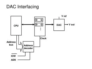
8051 – Address Bus De-mutiplexing • ALE – Address Latch Enable • 8051 drives it high when address is available on AD[7,0] • ALE is used as the “Enable” signal for an external latch (74LS573 or 373) • P0 and P2 unavailable
8051 External Code Memory Access • 8051 devices can have either on-chip or external code ROM • Input pin EA decides which is used and PSEN is used to enable it. • EA is an active low input to 8051 • EA connected to GND (Low) means 8051 uses external memory for code • EA connected to Vcc (High) means 8051 uses on-chip ROM for code memory • PSEN – Program Store Enable, active low • Connect this to the OE (output enable) of external ROM device
Microprocessor Interfacing - Basics • Any CPU (8051) has • Address bus A[15:0] • Data bus D[7:0] • Control lines : ALE, PSEN, RD, WR • A Single Processor mP based system has one CPU and many devices interfaced to it • Only one Address bus and one data bus in a Single Processor system • ABUS and DBUS are common for all interfaced devices and the CPU
Microprocessor Interfacing (contd.) • All Microprocessor compatible devices have enable lines (CE - Chip Enable or CS – Chip Select) • A function of the address bus f(A[15:0]) is connected to the CE of every device interfaced • This function is unique for every interfaced device • The CPU accesses each interfaced device by way of this unique function • This function is commonly referred to as the address of the device
Microprocessor Interfacing (contd.) • Interfaced devices either READ or WRITE or do BOTH on the DBUS. • Only one device has “exclusive access” • Achieved by using Tri-State buses • Devices that WRITE to DBUS have CE and RD/OE only • Read Cycle: Assert CE and then assert RD/OE • Devices that READ and WRITE to DBUS have CE, RD/OE and WR • Write Cycle: Assert CE and then assert WR
8051 Code Memory Read Cycle • 12MHZ part 87C51BH • TLLIV – ALE low to valid Instr 234ns max • TPLIV – PSEN low to valid Instr 145ns max • TAVIV – Addr valid to valid Instr 312ns max • TPLPH – PSEN pulse width 205ns min
8051 Data Memory Read Cycle • TRLDV – RD Low to valid Data 252ns max • TAVDV – Addr valid to valid Data 585ns max • TLLDV – ALE low to valid Data 517ns max • TRLRH – RD pulse width 400ns min
8051 – Address Generation • Address Generator is a piece of hardware that produces unique addresses to each interfaced device • Example • F1 = A15 . A14 • F2 = A15 . A14 • F3 = A15 . A14
What is needed ? • Need to know the following for all the devices before address generator can be designed • Base address of each device • Where it starts in the address map • Size of the device • How much of the address space it uses up
Example –1 : 2K Memory at 0x0000 • Pins : address – A10 to A0, Data – D7 to D0, RD, WR, CE • Base address = 0x0000 • Size = 2k (2 *1024 = 2048 bytes = 0x0800) • Address Map occupancy • 0x0000 to 0x07FF that is, • 0000 - 0000 - 0000 - 0000 binary to • 0000 - 0111 - 1111 - 1111 binary • 11 lowest address bits A10 to A0 have to be connected to the address pins on the memory
Example –1 : (contd.) • Unused address bits are • A15 to A11 • Base address is 0x0000 • CE has to be generated if all the unused address bits are logic-0 • CE is active low • CE = A15 + A14 + A13 + A12 + A11 • Then connect RD and WR
Example 2: Same Memory at 0x4000 • Base address is 0x4000 • 0100 0000 0000 0000 • Size is 2K • Unused address bits • A15 to A11 • CE has to be generated as per the truth-table • Expression is:
Complete vs. Partial Address Decoding • Complete address decoding: • Use all unused address bits to generate CE • Partial addressing decoding • Use a sub-set of the unused address bits • Used to reduce the address generator complexity • Produces address mirrors (same device at multiple addresses) • Example • 2K memory at 0x0000, we used A15 to A11 • Instead just connect A11 to CE • Same 2K memory device will then be mirrored for all values of A15 to A12 • 0x0000, 0x1000, 0x2000, 0x3000, …. , 0xF000 • Address generator became very simple, but we lost a lot of address space
74138 Decoder for Address Generation • 3 to 8 decoder, available in a single DIP package. • Takes 3 address lines and generates complete addressing among those • Example • Connect A15, A14, A13 to the decoder inputs • Decoder outputs give base addresses for • 0x0000, 0x2000, 0x4000, 0x6000,0x8000, 0xA000, 0xC000, 0xE000 • For more complicated address decoding: • Play tricks with 74138 enable connections. • Use programmable devices like PALs, PLDs or FPGAs
External Pure Code Memory • Could be RAM or ROM • Address generation as per standard procedure • Connect PSEN to the OE of the memory device • RD and WR are ignored • Connect Data bits D7-D0 of the memory and the 8051
External Code + Data Memory • Address generation as per standard procedure • Logically AND PSEN and RD and then connect to the OE of the memory • Connect WR from the 8051 to WR of the memory • Connect Data bits D7-D0 of the memory and the 8051
External I/O Devices • Same procedure as for interfacing memory • Only difference is that these devices have smaller sizes and use smaller portions of the address space • Example: • 8 LEDS connected to an 8-bit latch. The latch is address mapped to 0xF000. Size is 1byte • 8255 I/O device memory mapped at 0xD000. Size is 4 bytes
8051 - Switch On IO Ports • Case-1: • Gives a logic 0 on switch close • Current is 0.5ma on switch close • Case-2: • Gives a logic 1 on switch close • High current on switch close • Case-3: • Can damage port if 0 is output
DIP Switches on IO port • DIP switches usually have 8 switches • Use the case-1 from previous page • Can use a Resistor Pack, instead of discrete resistors
LED on IO Port • Try to use current sinking • Case-1 • LED is ON for an output of zero • Most LEDs drop 1.7 to 2.5 volts and need about 10ma • Current is (5-2)/470 • Case-2 • Too much current • Failure of Port or LED • Case-3 • Not enough drive (1ma) • LED too dim • Seven Segment LEDs • Common Anode/ Cathode • CA preferred • Case-1 may have LEDs of different brightness
8051 Interfacing with the 8255 • 8255 - Widely used I/O chip • 40 pins • Provides 3 eight bit ports PA, PB and PC • Port PC can be used as two 4 bit ports PCL and PCU • Ports have handshaking ability • Two address lines A0, A1 and a Chip select CS • Address space of 4 bytes • 00b selects Port A • 01b selects Port B • 10b selects Port C • 11b selects an internal control register • Read only.
8255 Functional Diagram • CS is used to interface with 8051 • If CS is generated from lets say Address lines A15:A12 as follows,A15:A12 = 1000 • Base address of 8255 is • 1000 xxxx xxxx xx00b • 8000H • Address of the registers • PA = 8000H • PB = 8001H • PC = 8002H • CR = 8003H
8255 Operating Modes • Mode 0 : Simple I/O • Any of A, B, CL and CU can be programmed as input or output • Mode 1: I/O with Handshake • A and B can be used for I/O • C provides the handshake signals • Mode 2: Bi-directional with handshake • A is bi-directional with C providing handshake signals • B is simple I/O (mode-0) or handshake I/O (mode-1) • BSR (Bit Set Reset) Mode • C alone is available for bit mode access • Allows single bit manipulation for control applications.
8255 Configuration • Configured by writing a control-word in CR register • CR definition • D7 : 1I/O mode, 0 BSR • D6,D5 : Mode selection for A and CU • 00 Mode0, 01 Mode1, 1x Mode2 • D4 : Port A control • 1 A input, 0 A output • D3 : Port CU control • 1 CU input, 0 CU output • D2 : Port B Mode selection • 0 B is in mode 0, 1 B is in mode 1 • D1 : Port B control • 1 B input, 0 B output • D0 : Port CL control • 1 CL input, 0 CL output • Refer to 8255 datasheet for additional options
8255 Usage: Simple Example • 8255 memory mapped to 8051 at address 8000H base • PA = 8000H, PB = 8001H, PC = 8002H, CR = 8003H • Control word for all ports as outputs in mode0 • CR : 1000 0000b = 80H • Code segment test: mov A, #80H ; control word mov DPTR, #8003H ; address of CR movx @DPTR, A ; write control word mov A, #55h ; will try to write 55 and AA alternatively repeat: mov DPTR, #8000H ; address of PA movx @DPTR, A ; write 55H to PA inc DPTR ; now DPTR points to PB movx @DPTR, A ; write 55H to PB inc DPTR ; now DPTR points to PC movx @DPTR, A ; write 55H to PC cpl A ; toggle A (55AA, AA55) acall MY_DELAY ; small delay subroutine sjmp repeat ; for (1)
BSR Mode • If used in BSR mode, then the bits of port C can be set or reset individually.
Interfacing the MCS-51 to: 7 and 16 segment displays a Multiplexed 7-Segment Display a Keypad an LCD
a f b g e c d The 7-Segment Display • The 7-segment display is nothing but 7 LEDs arranged to form the figure 8. • By turning on and off the appropriate segments (LEDs), different combinations can be produced. • The 7-segment display is useful for displaying the digits 0 through 9, and some characters. • However, it would be difficult to distinguish between things like a D and a 0.
The 7-segment Display (Contd.) • 7-segment displays come in 2 configurations: Common Anode Common Cathode • As we have seen when we discussed interfacing the basic LED, it would be preferable to connect the cathode of each diode to the output pin. • Therefore, the common anode variety would be better for our interfacing needs.
Interfacing a 7-segment display to the 8051 • Also, as seen with interfacing the LED, a resistor will be needed to control the current flowing through the diode. • This leaves two possibilities: • Case 2 would be more appropriate as case 1 will produce different brightness depending on the number of LEDs turned on.
The 16-segment Display • Similar to the 7-segment display except that it contains 16 LEDs. • With the 16 segments, it is possible torepresent all digits and letters in the alphabet (English). • With 16 LEDs, the 16-segment display requires 16 pins and 16 bits to determine the exact character. • All 16 values must be present at the same time. • Therefore, interfacing to a 16-segment display will require: • Either external hardware such as a latch. • Using two of the 8051 ports for connecting to a single display.
Multiplexed Displays • 7-segment displays require a lot of power (~10 mA per LED) and a large number of pins (8 per LED). • Suppose that a battery-powered system has 10 displays. • If the system is displaying “8888888888”. • All LEDs are on in all displays. • The total current required just to activate the displays is ~700 mA. • This would reduce the useful battery lifetime to a few hours at best. • The solution is not to activate all displays at once.
a b c d e f g Multiplexed Displays • The figure below show a 4 character multiplexed display. • The LED inputs are common to all 4 but each character has a separate “enable” input. • When a particular display is to be activated, its enable input is turned on, the display now uses the values on the LED pins to determine which LEDs to activate. • Total number of pins: 8 + # of characters.
Interfacing to a Multiplexed Display • To use a multiplexed display, each character will be flashed for a short period of time, • the first character is activated for a brief amount of time, then it is turned off. • Then the next character and so on through the four characters. • Back to the first character. • Only one character is activated at any point in time. • Worst case current requirement: ~70 mA. • If the multiplexing is done fast enough, the human eye will filter out the flickering and it would look like all the displays are one constantly. • Most humans cannot distinguish flashes at more than 20 per second. They would consider that to be steady light. • The scanning frequency should be at least 30 Hz. • Each character is on for 1/30 of a second.
The Program MOV B, #11H ; Display sequence LOOP: MOV R2, #04 ; Number of characters MOV R0, #20H ; Location of message NEXT: MOV P0, #00H ; Turn off the displays MOV A, @R0 ; Get the next character LCALL CONVRT ; Binary to 7-segment MOV P1, A ; Display the first character INC R0 ; Next character in the message MOV P0, B ; Turn on the appropriate display MOV A, B ; Go on to next display RL A MOV B, A LCALL DELAY ; On-time (1/30 seconds) DJNZ R2, NEXT ; Next character JMP LOOP ; Start next scan
Interfacing a Keypad • A 16-key keypad is built as shown in the figure below. • 16 keys arranged as a 4X4 matrix. • Must “activate” each row by placing a 0 on its R output. • Then the column output is read. • If there is a 0 on one of the column bits, then the button at the column/row intersection has been pressed. • Otherwise, try next row. • Repeat constantly.
Interfacing a Keypad • Algorithm: • Drive a “0” on a row • Read all the columns • If any key had been pressed, its column will be “0”, else 1 • Keep repeating in a loop for each successive row • Example: • Switch 4 is pressed • R1 0, C1:C4 = 1111 • R2 0, C1:C4 = 0111 • Switch 2 is pressed • R1 0, C1:C4 = 1101
Bouncing Contacts • Push-button switches, toggle switches, and electromechanical relays all have one thing in common: contacts. • These metal contacts make and break the circuit and carry the current in switches and relays. Because they are metal, contacts have mass. • Since at least one of the contacts is on a movable strip of metal, it has springiness. • Since contacts are designed to open and close quickly, there is little resistance (damping) to their movement.
Bouncing • Because the moving contacts have mass and springiness with low damping they will be "bouncy" as they make and break. • That is, when a normally open (N.O.) pair of contacts is closed, the contacts will come together and bounce off each other several times before finally coming to rest in a closed position. • The effect is called "contact bounce" or, in a switch, "switch bounce”.
Why is it a problem? • If such a switch is used as a source to an edge-triggered input such as T0 or INT0, then the MCS-51 will think that there were several “events” and respond several times. • The bouncing of the switch may last for several milliseconds. • Given that the MCS-51 operates at microsecond speed, a short ISR may execute several times in response to the above described bounciness.
Hardware Solution • The simplest hardware solution uses an RC time constant to suppress the bounce. The time constant has to be larger than the switch bounce and is typically 0.1 seconds. • The buffer after the switch produces a sharp high-to-low transition. • If the button is pushed again before the expiration of the time constant, the second press will not be recognized.
Software Solution • It is also possible to counter the bouncing problem using software. • This would require one of two approaches: • Delays: When the first edge is noticed, an “appropriate” delay is executed, then the value of the line is checked again to make sure the line has stopped bouncing. • Actually, it is also necessary to execute a similar delay on the button’s release to counter the release bouncing. • Interrupts and Timers: When the first edge is noticed, a timer is started. When following edges appear, the value of the counter is checked. If the edges appear “too quickly”, they will be rejected.