Lecture #19
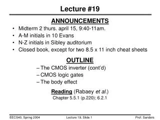
Lecture #19. ANNOUNCEMENTS Midterm 2 thurs. april 15, 9:40-11am. A-M initials in 10 Evans N-Z initials in Sibley auditorium Closed book, except for two 8.5 x 11 inch cheat sheets OUTLINE The CMOS inverter (cont’d) CMOS logic gates The body effect Reading (Rabaey et al. )

Lecture #19
E N D
Presentation Transcript
Lecture #19 ANNOUNCEMENTS • Midterm 2 thurs. april 15, 9:40-11am. • A-M initials in 10 Evans • N-Z initials in Sibley auditorium • Closed book, except for two 8.5 x 11 inch cheat sheets OUTLINE • The CMOS inverter (cont’d) • CMOS logic gates • The body effect Reading(Rabaey et al.) Chapter 5.5.1 (p.220); 6.2.1
Features of CMOS Digital Circuits • The output is always connected to VDD or GND in steady state • Full logic swing;large noise margins • Logic levels are not dependent upon the relative sizes of the devices (“ratioless”) • There is no direct path between VDD and GND in steady state • no static power dissipation
i i The CMOS Inverter: Current Flow during Switching N: sat P: sat VOUT N: off P: lin C V DD VDD S G N: sat P: lin D VIN VOUT B D E A D G N: lin P: sat S N: lin P: off 0 VIN VDD 0
VDD-VT VT Ipeak 0 tsc Energy consumed per switching period: Power Dissipation due to Direct-Path Current VDD V DD vIN: S G 0 D i vIN vOUT D G i: S time
N-Channel MOSFET Operation An NMOSFET is a closed switch when the input is high A B A B Y Y X X Y = X if A and B Y = X if A or B NMOSFETs pass a “strong” 0 but a “weak” 1
P-Channel MOSFET Operation A PMOSFET is a closed switch when the input is low A B A B Y Y X X Y = X if A and B = (A + B) Y = X if A or B = (AB) PMOSFETs pass a “strong” 1 but a “weak” 0
Pull-Down and Pull-Up Devices • In CMOS logic gates, NMOSFETs are used to connect the output to GND, whereas PMOSFETs are used to connect the output to VDD. • An NMOSFET functions as a pull-down device when it is turned on (gate voltage = VDD) • A PMOSFET functions as a pull-up device when it is turned on (gate voltage = GND) VDD A1 A2 AN Pull-up network input signals PMOSFETs only … F(A1, A2, …, AN) A1 A2 AN Pull-down network NMOSFETs only …
CMOS NAND Gate VDD A B F A B
CMOS NOR Gate VDD A B F A B
CMOS Pass Gate A Y Y = X if A X A
The “Body Effect” VTis a function of VSB: g is the body effect coefficient When the body-source pn junction is reverse-biased, |VT| increases. Usually, we want to minimizeg so that IDsat will be the same for all transistors in a circuit.

