Download
1 / 23
300 likes | 637 Vues
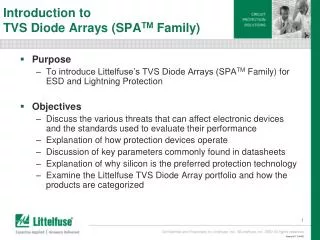
Introduction to TVS Diode Arrays (SPA TM Family). Purpose To introduce Littelfuse’s TVS Diode Arrays (SPA TM Family) for ESD and Lightning Protection Objectives Discuss the various threats that can affect electronic devices and the standards used to evaluate their performance

E N D
Introduction to TVS Diode Arrays (SPATM Family) • Purpose • To introduce Littelfuse’s TVS Diode Arrays (SPATM Family) for ESD and Lightning Protection • Objectives • Discuss the various threats that can affect electronic devices and the standards used to evaluate their performance • Explanation of how protection devices operate • Discussion of key parameters commonly found in datasheets • Explanation of why silicon is the preferred protection technology • Examine the Littelfuse TVS Diode Array portfolio and how the products are categorized
ElectroStatic Discharge Protection Lightning AC Power Contact Sustained Overload ESD is one of four major threats to electronic equipment and is the direct result of human interaction.
What is ESD and where does it come from? – Triboelectric Charging • Triboelectric charging occurs when two materials make contact and separate • Electrons from one material are transferred to another leaving one positively charged and the other negatively charged. • The nature of the materials will determine who losses or gains electrons • The build up of static electricity is determined by several factors such as: area of contact, the speed of separation, relative humidity, and chemistry of the materials, surface work function, etc. *Table from ESDA
ESD Standards – Human Body Model, MIL-STD • Based on Skin-to-Metal Contact • e.g. Person touches pin of IC, discharging directly to pins • Referenced in the Military Standard (883, Method 3015.7) test specification • Addresses the Manufacturing/Production environment; testing is done directly on the IC • Circuit Model: VoltagePeak Current 500V 0.33A 1,000V 0.67A 2,000V 1.33A 4,000V 2.67A 8,000V 5.33A
ESD Standards – IEC 61000-4-2 • Based on Metal-to-Metal Contact • e.g. Person with tool/key in hand discharges to I/O port • Used in IEC 61000-4-2 test specification • Addresses the user-environment; testing is done at the application or system level • Circuit Model: VoltagePeak Current 2,000V 7.5A 4,000V 15.0A 6,000V 22.5A 8,000V 30.0A
ESD Standards – IEC 61000-4-2 Waveform • Discharge VoltageFirst PeakCurrent, 30nsCurrent, 60ns • 2,000 V7.5 A 4 A 2 A • 4,000 V 15.0 A 8 A 4 A • 6,000 V 22.5 A 12 A 6 A • 8,000 V 30.0 A 16 A 8 A • Specified current values, per discharge voltage Most all manufacturers test to 8kV or higher!
Comparing the Two Specifications– IEC 61000-4-2 vs. Human Body Model Peak current Peak current Discharge VoltageHuman Body ModelIEC 61000-4-2 500 V 0.33 A 1,000 V 0.67 A 2,000 V 1.33 A 7.5 A 4,000 V 2.67 A 15.0 A 8,000 V 5.33 A 30.0 A • The key here is that a chipset that survives Human Body Model testing (in the manufacturing environment) is not guaranteed to survive in the field, where the exposure to ESD will be much more severe. • Different models yield much different peak current values; ultimately electrical stresses on the chipset are very different. • ESD levels in the field far exceed the values that can be generated in the manufacturing environment.
TVS Diode Arrays for ESD and Lightning Protection • Generally, 2 circuit types • TVS Arrays • Typical capacitance range 3.5pF-30pF • ESD Level: ±8kV to ±30kV • Can be unidirectional or bidirectional • Diode Arrays • Typical capacitance range 0.40pF-5pF • ESD Level: ±8kV to ±30kV • Can be unidirectional or bidirectional • Sizes range from 0201 to MSOP-10 • Operating voltage up to 6VDC • Number of channels range from 1-14
TVS Diode ArraysHow do they work? Transient ESD Voltage GND Circuit Damage Level Clamping Level Normal Operating Level Time
TVS Diode ArraysHow do they work? Transient ESD Voltage Energy Dissipated in TVS GND Circuit Damage Level Clamping Level Normal Operating Level Time
TVS Diode ArraysWhat are the key parameters? +I +I I I PP PP I I T T I I R R - - V V +V +V V V V V V V R R BR BR C C - - I I Bidirectional Unidirectional +I +I I I PP PP I I T T I I R R - - V V +V +V V V V V V V R R BR BR C C - - I I
+I IPP IT IR -V +V VR or VRWM VBR VC -I Key Parameters: VR or VRWM Reverse Standoff Voltage or Reverse Working Maximum
+I IPP IT IR -V +V VR VBR VC -I Key Parameters: VBR Breakdown Voltage
+I IPP IT IR -V +V VR VBR VC -I Key Parameters: Vc Clamping Voltage
Key Parameters: Peak Pulse Current (IPP) • Peak Pulse Current (Lightning Capability) • For protection of telecom or broadband equipment lightning immunity is just as important as ESD protection so for these devices the peak pulse current can be the driving factor. • The required level is often driven by regulatory standards such as Telcordia GR-1089, ITU, YD/T, IEC, etc • Common waveshapes (trxtd) are 2x10µs, 8x20µs, and 10x1000µs
Key Parameters: Dynamic Resistance (RDYN) • The figure below depicts a protection device as a variable resistor which will be high impedance (low leakage) during normal circuit operation and low impedance during any EOS (Electrical Over Stress) or ESD event. • The ultimate goal of a protection device is to provide the lowest resistance shunt path to GND under an ESD event to minimize the energy seen by the chipset or IC. • Ideally, all current would be steered into the ESD device so that the protected IC would not have to dissipate any of the energy input into the circuit. • Lower RDYN = Lower clamping voltage = Better, more robust protection
Dynamic ResistanceHow it’s calculated • The dynamic resistance is the impedance value that the ESD suppressor represents as it switches from “off” to “on” • Using SP1005-01WTG as an example, we find: • This is the single best parameter to use in comparing ESD suppressors to determine which one is better!
Dynamic ResistanceComparison of Competing Technologies • Data of Littelfuse’s SP1003-01DTG vs. a competitor varistor. Both devices have the same footprint (0402), same standoff voltage, and similar capacitances. Peak Voltage = 240V vs. 156V Clamp Voltage = 75V vs. 16V The area between the curves represents the amount of energy that DOES NOT get to the chip when this MLV was replaced by the SP1003-01DTG. The reduction in transient energy helps ensure that the chipset will survive even severe ESD events.
Key Parameters: Capacitance • Capacitance • Low capacitance is needed in high-speed applications to minimize signal degradation • A low capacitance device ensures the eye-diagram can stay within spec to prevent data corruption
TVS Diode Arrays Product Categories • General Purpose ESD Protection • Low-speed circuits (< 100Mbps) • Examples include power ports, keypads, buttons, switches, audio, analog video, USB 1.1 • Low Capacitance ESD Protection • High-speed data buses (> 100Mbps) • Examples include HDMI, USB 2.0, USB 3.0, FireWire, DisplayPort, Ethernet, eSATA • Lightning Surge Protection • Specifically refers to Ethernet (10/100/1000) and xDSL circuits in which there is a requirement to provide ESD and/or lightning surge protection (will vary by standard, customer, and application).
TVS Diode Arrays Product Categories • General Purpose ESD Protection • Low Capacitance ESD Protection • Lightning Surge Protection SP05 SP1001 SP1002 SP1003 SP1004 SP1005 SP1006 SP1007 SP1010 SP1011 SP720 SP721 SP723 SP724 SP725 SP6001 SP6002 SP3001 SP3002 SP3003 SP3004 SP3010 SP3011 SP3012 SP03-3.3 SP03A-3.3 SP03-6 SPLV2.8 SPLV2.8-4 SP3050 SP4060 SP4061 SP4062 SP4040
System Level ESD Guide • Available on the Littelfuse website: • http://www.littelfuse.com/data/en/Technical_Articles/Littelfuse_ESD_System_Level_Guide.pdf • Discusses multiple applications such as: • USB1.1/2.0/3.0 • HDMI • DVI • 10/100/1000 Ethernet • eSATA • 1394a/b • LVDS • Audio (Speaker/Microphone) • Analog Video • SIM Sockets • RS-485 • CAN Bus • Keypad/Push button • LCD/Camera display interfaces