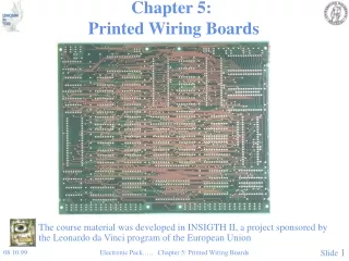
Printed Wiring Board Fabrication
280 likes | 801 Vues
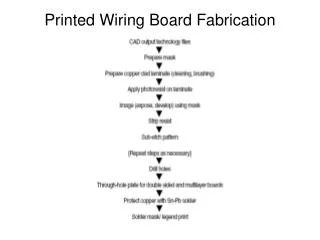
Printed Wiring Board Fabrication. Imaging. For feature sizes less than 200 μ m, use photolithography process Clean surface Apply photoresist Expose photoresist Develop photoresist image Pattern transfer image (plating or etching) Strip photoresist

Printed Wiring Board Fabrication
E N D
Presentation Transcript
Imaging • For feature sizes less than 200μm, use photolithography process • Clean surface • Apply photoresist • Expose photoresist • Develop photoresist image • Pattern transfer image (plating or etching) • Strip photoresist • Dry film photoresist for pattern formation • Liquid photoresists for precision work (less than 50μm)
Drilling • Purpose is to form an electrical connection between layers and permit through-hole component mounting • Typically use tungsten carbide drill bits at speeds of 50,000 to 100,000rpm • Most common defects are: • Delamination - vibrational • Smear - thermal • Burr - sharpness • Debris - sharpness • Drill smear is the most important factor for hole quality • Drill smear occurs due to heating of the PWB by the drill, which can cause epoxy-resin melting
Plating • Metal deposition by electroless and electrolytic processes • Typically use copper with the following requirements • High electrical conductivity • Good mechanical strength • High ductility and elongation • Excellent solderability • Good tarnish and corrosion resistance • Good etchant resistance • Also can add Sn, Sn-Pb, or Ni undercoating as a solder barrier
Etching • Typically chemical etching used (alkaline ammonia, hydrogen peroxide-sulfuric acid, cupric cholride) • Process steps: • Resist stripping • Precleaning • Etching • Neutralization • Water rinsing • Drying
Single-sided PWB Fabrication • Single layer process shown • Can either use: • Photolithographic process • Higher precision • Higher cost • Screen printing • Lower precision • Lower cost
Double-sided PWB Fabrication • Holes drilled, deburred, and cleaned • Panels prepared for electroplating • Deposit, mask, expose, and develop photoresist (UV light) • Copper electroplating • Additional electroplating (Sn-Pb) to protect and improve quality of surface • Strip photoresist • Solder reflow
Multilayer PWB Fabrication • Pressing process to form layers • Alignment is critical • Process steps: • Panels produced using double-sided etching from prepreg laminates • Panels are laminated, pressed, and cured • Additional drilling, electroplating and etching as required
Solder Masks • Three primary types of solder resist masks: • Screen-printed • Dry film • Liquid photoimageable (LPI) • Dry film and LPI produce finer features than screen-printed • Protection of exposed surfaces using finishes
Limitations on PWB Process • New products require higher pad densities • Drilled hole technology becomes too expensive • Microvia is the solution
Microvias • Fabrication processes: • Laser drilling • Plasma or RIE • Photolithography • Advantages for high volume production: • Increased circuit density • Advanced packages enabled • Better electrical performance • Improved reliability than drilled holes • Improved thermal conductance • Lower PWB cost
Microvia Generation • Photovia • Utilizes photolithography • Requires photosensitive permanent dielectrics • Plasmavia (PEV) • Very flexible process • Can generate many different geometries • Typically 60-90μm diameter • Laservia • Economical for mass production • Nd:YAG, CO2, UV excimer • Paste-via • Cheap, but less reliable
Laservia is the best overall microvia process • Direct CO2 laser drilling is leading throughput and quality of holes • 20,000 holes/min/head
Microvia Board Technologies • Three major technologies • Surface Laminar Circuitry (SLC) or Build-Up Technology • All Layer Internal Via Hole (ALIVH) Technology • Buried Bump Interconnection Technology (B2IT)
Build-Up Technology • Can use photosensitive dielectrics for photovias or use lasers to drill vias • Copper lines can be spaced as close as 20μm wide • Lastly, gold plating is used for wire bondable surface finish
All Layer Internal Via Hole (ALIVH) Process • Invented by Matsushita in Japan • Used primarily for cell phone boards • Uses epoxy-aramid prepregs with laser drilled vias, which are filled with copper paste
Buried Bump Interconnection Technology (B2IT) • Invented by Toshiba in Japan • Uses silver paste bumps to punch holes in dielectric or prepreg
PWB Market Expected growth of PWBs and microvias
PWB Trends Feature size and pitch decrease as number of pins increases
Summary and Future Trends • PWB Fabrication process (Imaging, Drilling, Plating, and Etching) • Different board fabrication processes (Single-sided, Double-sided, and Multilayer) • Microvia generation (Photovia, Plasmavia, and Laservia) • Microvia board fabrication (Build-up, ALIVH and B2IT) • Trade-offs (cost, reliability, quality of contacts, dielectric properties, feature sizes, etc.)