Download
1 / 5
50 likes | 161 Vues
Technology drive today many things has been replaced with better design and technique. The research throughout designing and constructing of Capacitive Discharge Ignition CDI system for Spark Ignition SI Engine which is based on electronic ignition and contact point ignition. CDI system is composed of pulse generation circuit, pulse control circuit, main charge and discharge capacitor coil and spark plug. Mainly composed of pulse control circuit and pulse generation circuit which main function is to generate DC high voltage when the DC 12V supply from car battery. Pulse control circuit generates the pulse to control oscillator on and off state and trigger gate drive pulse to the SCR. When the SCR from pulse control circuit open, the main capacitor discharge high voltage 300V from pulse generation to ignition coil. The coil generates high voltage 25 30kV which it depends on number of turn ration from coil primary and secondary winding. System is divided into ten blocks. The operation and function of each block is mentioned in detail. Design calculations for inverter, rectifier and selection of SCR, analyzing of components are highlighted for system. Su Su Yi Mon "Capacitive Discharge Ignition (CDI) System for Spark Ignition (SI) Engine (Pulse Control Circuit)" Published in International Journal of Trend in Scientific Research and Development (ijtsrd), ISSN: 2456-6470, Volume-3 | Issue-5 , August 2019, URL: https://www.ijtsrd.com/papers/ijtsrd26773.pdf Paper URL: https://www.ijtsrd.com/engineering/electronics-and-communication-engineering/26773/capacitive-discharge-ignition-cdi-system-for-spark-ignition-si-engine-pulse-control-circuit/su-su-yi-mon<br>

E N D
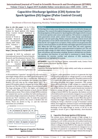
International Journal of Trend in Scientific Research and Development (IJTSRD) Volume 3 Issue 5, August 2019 Available Online: www.ijtsrd.com e-ISSN: 2456 – 6470 Capacitive Discharge Ignition (CDI) System for Spark Ignition (SI) Engine (Pulse Control Circuit) Su Su Yi Mon Department of Electronic Engineering, Mandalay Technological University, Mandalay, Myanmar How to cite this paper: Su Su Yi Mon "Capacitive Discharge Ignition (CDI) System for Spark Ignition (SI) Engine (Pulse Control Circuit)" Published in International Journal of Trend in Scientific Research and Development (ijtsrd), ISSN: 2456- 6470, Volume-3 | Issue-5, August 2019, pp.1925-1929, https://doi.org/10.31142/ijtsrd26773 Copyright © 2019 by author(s) and International Journal of Trend in Scientific Research and Development Journal. This is an Open Access article distributed under the terms of the Creative Commons Attribution License (CC (http://creativecommons.org/licenses/by /4.0) A CDI module has "capacitor" storage of its own and sends a short high voltage (about over 300V) pulse through the coil. The coil now acts more like a transformer (instead of a storage inductor) and multiplies this voltage even higher. Modern CDI coils step up the voltage about 100:1. So, a typical CDI module output is stepped up to over 30kV output from the coil. The CDI output voltage of course can be higher. The huge advantage of CDI is the higher coil output and "hotter" spark. The spark duration is much shorter (about 300ms) and accurate. This is better at high RPM (revolution per minute) but can be a problem for both starting and/or lean mixture/high compression situations. CDI systems can and do use "low" resistance coils. To study the capacitive discharge ignition system, the circuit is divided into ten blocks. These are shown in Fig. 1.1 and the overview operations are as follows. ABSTRACT Technology drive today many things has been replaced with better design and technique. The research throughout designing and constructing of Capacitive Discharge Ignition (CDI) system for Spark Ignition (SI) Engine which is based on electronic ignition and contact point ignition. CDI system is composed of pulse generation circuit, pulse control circuit, main charge and discharge capacitor coil and spark plug. Mainly composed of pulse control circuit and pulse generation circuit which main function is to generate DC high voltage when the DC 12V supply from car battery. Pulse control circuit generates the pulse to control (oscillator on and off state) and trigger gate drive pulse to the SCR. When the SCR from pulse control circuit open, the main capacitor discharge high voltage 300V from pulse generation to ignition coil. The coil generates high voltage 25-30kV which it depends on number of turn ration from coil primary and secondary winding. System is divided into ten blocks. The operation and function of each block is mentioned in detail. Design calculations for inverter, rectifier and selection of SCR, analyzing of components are highlighted for system. KEYWORDS: Capacitive Discharge Ignition; monostable mode, Contact Point Ignition System, Electrionic Ignition System INTRODUCTION Capacitive Discharge Ignition (CDI) is most widely used today an automotive and marine engines. IJTSRD26773 BY 4.0) In figure1, pulse generation circuit is to generate the high voltage pulse using dc to ac voltage inverter, ac to dc voltage rectifier, and charge main capacitor. The pulse control circuit is to control the pulse generation circuit and trigger to the SCR using switching and trigger transistors. This system stores electrical energy of high voltage in a capacitor until the trigger releases the charge to the primary winding of a coil. In this system the coil is a pulse transformer instead of being an energy-storage device as is normal. To obtain a voltage of about 400V for the capacitor, the battery current is first delivered to an inverter(to change d.c to a.c) and then it is passed to a transformer to raise the voltage and to get dc voltage, full wave bridge rectifier is used. When the spark is required, the trigger releases the energy to the coil primary winding by 'firing' a thyristor (a type of transistor switch which, once triggered, continues to pass current through the switch even after the trigger current has ceased). Suddenly discharge of the high-voltage in excess of 30 kV in the secondary circuit to give a high-intensity, short-duration spark. A.Capacitive Discharge Ignition (CDI) System The system stores electrical energy of high voltage in a capacitor until the trigger releases the charge to the primary winding of a coil. In this system the coil is pulse transformer instead of being an energy-storage device as is normal. To obtain a voltage of about 400V for the capacitor the battery current is first delivered to an inverter (to change d.c to a.c) and then it is passed to a transformer to raise the voltage. When the spark is required the trigger releases the energy to Figure1 Block Diagram of Capacitive Discharge Ignition System @ IJTSRD | Unique Paper ID – IJTSRD26773 | Volume – 3 | Issue – 5 | July - August 2019 Page 1925
International Journal of Trend in Scientific Research and Development (IJTSRD) @ www.ijtsrd.com eISSN: 2456-6470 the coil primary winding by 'firing' thyristor. Sudden discharge of the high-voltage energy to the primary winding causes a rapid build-up in the magnetic flux of the coil and induces a voltage in excess of 40kV in the secondary circuit to give a high-intensity, short-duration spark. Although the CDI system is particularly suited to high-performance engines, spark duration of about 0.1 ms given by this system is normally too short to ignite reliably the weaker petrol-air mixtures used with many modern engines. To offset the problem of the short spark duration, advantages are sometimes taken of the high secondary output by increasing the sparking plug gap to give a larger spark. Although the system can be triggered by a mechanical breaker, the advantages of a pulse generator, using either inductive or Hall Effect, makes this type more attractive. The short charge-up time overcomes the need for dwell-angle control because charge time of a CDI system is independent of engine speed. Although the external appearance of an ignition transformer of a CDI system is similar to normal ignition coil, the internal construction is quite different. As the ignition transformer and capacitor form an electrically tuned circuit, it is necessary to fit the recommended type of transformer when replacement is required. Although a standard coil used in place of an ignition transformer will operate without damaging the system, many of the advantages of a CDI system are lost. Conversely, damage to control module and transformer will occur immediately the system is used. The CDI principle is also used in some small engines as fitted to motor cycles, lawn mowers, etc. A battery is not used in these cases, so the energy needed by the CDI system is generated by a magneto. B.Spark Ignition System The purpose of spark ignition system is to provide, at the correct moment in relation to piston travel and rpm, one or more electrical sparks such that the fuel-air mixture in the combustion chamber may be ignited at one or more places. Most commonly, the sparks are produced at the combustion chamber end of a 'spark plug'. The higher the pressure in the combustion chamber at the time of ignition, the higher the voltage needed to jump the spark plug gap. At around the same time that magneto's were in use, there were wooden boxes with a vibrating electrical contact which sent storage battery energy into a coil of wire, said wire wound on an iron core. Since the vibrating contact opened and closed the circuit rapidly, the coil input winding was nearly continuously interrupted. Each time the contact closed, the coil charged up magnetically, and each time the contact opened, the coil transformed that energy into high voltage. There was a separate wire winding on that iron core, with many hundreds of times more turns, and those extra turns' transformed the lower voltage of the battery to a few thousand volts or more, and this was applied to rather crude looking spark plugs. In many very early cars, that spark was applied continuously. The biggest problem with the vibrating contact system is that the spark output is constantly flowing, and it is hard to "time' the combustion event, even with a rotating contact distributor. This was not a big problem with very low output engines with very low rpm and compression ratios. The ignition system supplies high-voltage surges (as high as 30kV) of current to the spark plugs in the engine cylinders. These surges produce electric sparks at the spark-plug gaps. The sparks ignite, or set fire to, the compressed air-fuel mixture in the combustion chambers. Each spark appears at the plug gap just as the piston approaches top dead center on the compression stroke, when the engine is idling. At higher speed or during part-throttle operation, the spark is advanced. It occurs somewhat earlier in the cycle. The mixture thus has ample time to burn and deliver its power. There are two general types of ignition system. They are (a) Contact Point Ignition System (b) Electronic Ignition System. C.Capacitive Discharge Ignition for Low Emission In low emission Capacitive Discharge Ignition system circuit, there are main two portions. They are A.Pulse control circuit, B.Pulse generation circuit. In the pulse control circuit, in figure 2, the switching circuit used switching PNP and NPN transistors and triggering circuit used 555 IC as monostable. Components using in the circuit are 2N2219 NPN transistor (similar C1815), as switching, 2N2907 PNP transistor, as switching, 555 timer, as monostable, SCR (HEPR1223), 1N914 diodes, Resistors and Capacitors. Electronic ignition system does not use contact points. Instead, it uses a magnetic pick-up device in the distributor and an electronic amplifying device with transistors. When the cap on, the distributor looks the same as the contact point distributor. The CDI is designed both two systems. So it has electronic amplifying device and distributor contact point. The design of pulse control circuit consists of switching, triggering and selection of SCR and SCR snubber circuits. Pulse control portion in CDI system is mainly performed to control the pulse generation circuit and to generate gate pulse for SCR. When the distributor point open, switching transistors turn on and off state and triggers 555 timer. 555 timer performs as monostable and that provides gate drive pulse for SCR and control to on and off oscillator with 555 astable. Capacitive Discharge Ignition (CDI) system is an important role for Spark Ignition (SI) engine. Most of the Spark Ignition car engine used contact point system for high voltage to distributor to get spark. CDI system in this thesis is composed of contact point and electronic ignition system. Figure 2 Overall Complete Circuit Diagram @ IJTSRD | Unique Paper ID – IJTSRD26773 | Volume – 3 | Issue – 5 | July - August 2019 Page 1926
International Journal of Trend in Scientific Research and Development (IJTSRD) @ www.ijtsrd.com eISSN: 2456-6470 output converts to low. In this way, the timer operating in the monostable repeats the above process. It must be noted that, for a normal operation, the trigger pulse voltage needs to maintain a minimum of Vcc/3 before the timer output turns low. That is, although the output remains unaffected even if a different trigger pulse is applied while the output is high, it may be effected and the waveform does not operate properly if the trigger pulse voltage at the end of the output pulse remains at below Vcc/3. Figure 4 shows such a timer output abnormality. E.Design of Switching Circuit from Pulse Control Circuit In proposed pulse control circuit, transistors perform as switching transistors. When the point from distributor open, transistor is turns on and triggered. Figure3 Internal Block Diagram of 555 Timer The 555 timer has two basic operational modes: one shot and astable. In the one-shot mode, the 555 is called a monostable multivibrator. The monostable circuit generates a single pulse of fixed time duration each time it receives and input trigger pulse. Thus it is named one-shot. If there is no triggering input, the circuit stays in its stable conditionwhich is the off-state. The output stays at zero. Whenever it is triggered by an inputpulse, the monostable switches to its temporary state. It remains in that state for a periodof time determined by an RC network. It then returns to its stable state.In other words; a monostable multivibrator operates by charging a capacitor with a current set by an external resistance. D.555 Monostable Operation In the Monostable Operation mode, the timer generates a fixed pulse whenever the trigger voltage falls below Vcc/3. When the trigger pulse voltage applied to the trigger pin falls below Vcc/3 while the timer output is low, the timer's internal flip-flop turns the discharging Tr. off and causes the timer output to become high by charging the external capacitor C1 and setting the flip-flop output at the same time. The voltage across the external capacitor C1, VC1 increases exponentially with the time constant t=RA*C and reaches 2Vcc/3 at td=1.1RA*C1 Figure 5 Operation Circuit for Q7 I1 = VBE/R10 = 1.5mA -Vin + I1R9 + I1R10 = 0, the Vin = I1R9 +I1R10 = 1.41V Assumed IC = 90 mA (from C1815 = 2N2219A datasheet) For saturation, RC = (VCC – VCE(sat)) / IC(sat) = 132Ω So, RC = R11 =100Ω is choosen. For switching transistors, IB = 0.1IC = 90mA When Q7 is forward biased (get IB current), turned on. And then, VOUT = VCC - ICRC = 3V So, VOUT=3V triggered to M2. From test condition, the trigger voltage from pin 2 is 3.6 V. Figure4 Monostable Circuit using R and C Hence, capacitor C1 is charged through resistor RA. The greater the time constant RAC, the longer it takes for the VC1 to reach 2Vcc/3. In other words, the time constant RAC controls the output pulse width. When the applied voltage to the capacitor C1 reaches 2Vcc/3, the comparator on the trigger terminal resets the flip-flop,turning the discharging Tr.on. At this time, C1 begins to discharge and the timer Figure6 Operation Circuit for Q8 @ IJTSRD | Unique Paper ID – IJTSRD26773 | Volume – 3 | Issue – 5 | July - August 2019 Page 1927
International Journal of Trend in Scientific Research and Development (IJTSRD) @ www.ijtsrd.com eISSN: 2456-6470 For switching transistor Q8, when Q7 is turns on, Q8 turns off. Therefore, Assumed IC=10mA RC = (VCC – VCE(sat)) / IC, (VCE(sat)= 0.1V) = 1.19kΩ So, we choose RC = R16 =1kΩ For switching transistors, IB = 0.1IC = 1mA VR15 = Vin - VBE, Vin = 10V Therefore, charging voltage in C7 is 10V. For switching transistor Q6, Therefore, VC1 increases exponentially with the time constant t, Where t = RA C1.µ So, = 100µs During this time, Input voltage of pin 2, V2< 4 ( VCC/3 ). C1 continues to charge until the voltage across it reaches 2/3Vcc, at which point the output of 555 goes low and C1 discharges through the resistor RA to pin 7. Therefore, = 110µs During this time, charging of voltage in C1, VC1 = 8V (2Vcc/3 ). The greater time constant t, the longer it takes for the VC1 to reach 2Vcc/3.This means that charging time is longer in C1. = 10k 0.01µ tdischarge = 1.1RAC1 Figure7 Operation Circuit of Q6 When the output of M2 high, Q6 turns off. Assume Vin = 7.3V RT = R20 + R19 = 4.4kΩ IB = Vin / RT = 1.65mA IB = 0.1IC, Therefore, IC = (1.65m / 0.1) = 20uA Vout = VCC - ICRC = 11.98V 12V This voltage applied to the pin 4 (reset) of the M1. So M1 is not active and can’t give pulse to inverter circuit. F.Design of Trigger Circuit By comparison, 555 monostable from Pulse Control Circuit, C1 = C11 = 0,01µF and RA= R28 = 10kΩ. During this time, transistor Q9 is turned on and VR27 have zero voltage (R27 parallel with short line). So R27 can neglect. Therefore, RA = R28 VC1 increase with time constant RA. When the trigger pulse applied to the 2 pin falls below VCC/3 while time output is low, the timer’s internal flip-flop turns the discharging transistor off and causes the timer output to become high by charging the external capacitor C11 and setting the flip-flops output to become high by charging the external capacitor C11. Figure9 Constructed CDI Circuit Figure 10 Constructed of Pulse Control Circuit Figure11 Trigger and output waveform of 555 M2 G.Conclusion and Disscussion Capacitive Discharge Ignition (CDI) system in this research is based on contact point and electronic ignition system. In contact point within the distributor system, rotation of the Figure 8 Equivalent 555 Monostable Circuit Using R and C @ IJTSRD | Unique Paper ID – IJTSRD26773 | Volume – 3 | Issue – 5 | July - August 2019 Page 1928
International Journal of Trend in Scientific Research and Development (IJTSRD) @ www.ijtsrd.com eISSN: 2456-6470 shaft and breaker cam causes the distributor contact points to open and close. The contact point close and open once for each cylinder with every breaker cam rotation. Thus one high voltage surge is produced by the ignition coil for each cylinder every two crankshaft revolution. SCR using in this project is high power and high current SCR, it has maximum 600V, 8A. Parallel capacitor commutation is used to turn off the SCR. It is protected with snubber circuit. In this research, the design and analyzing of pulse control circuit to generate high voltage in right time for engine have been described. In other CDI system, switching and triggering circuit used MOSFET replacing switching transistors and 555 timer. In local market, switching transistors and 555 timers are easily to buy and low cost for construction. So, the proposed control circuit is designed switching transistors and 555 timers for triggering. As a result, the proposed circuit is low cost, low emission and simple circuit to control the pulse for SCR and pulse generation circuit for spark ignition engine. It can be used not only spark ignition petrol engine but also spark ignition gas engine. References [1]Ashfaq Ahmed. 1999. “Power Electronic for Technology.” Purdue [3]Hiller. “Fundamentals of Automotive Electronics”, 2nd Edition [4]Lars Eriksson. “Spark Advance for Optimal Efficiency.”SAE Technical Paper No. 99-01-0548, 1999. [5]Lars Eriksson, Lars Nielsen, and Jan Nytomt. “Ignition Control byIonization Current Interpretation.”SAE SP- 1149, 1996. [6]Thomas, L. Floyd. 1996. “Electronic Device.” Prentice- Hall International (UK) limited. London. [7]Vithayathil Joseph 1995. “Power Electronic.”McGraw- Hill Series in Electrical and Computer Engineering. [8]http://www.datasheetarchive.com [9]http://www.alldatasheet.com [10]http://www.designews.com [11]http://www.automotivetechnology.co.uk [12]http://www.familycar.com [13]www.st.com [14]Prajyot Mehta, Dr. AshwiniBarbadekar. “Capacitive discharge ignition for two wheelers”, IJARECE, Vol 6, Dec 2017. [15]M. Santhosh Rani, Resonant Converter based Automobile Ignition system, International Journal of Pure and apply Mathematics, vol118, 2018 [2]Frederic A. Matekunas. “Engine Combustion Control with Ignition Timing by Pressure Ratio Management” US Pat., A, 4622939, Nov. 18 1986. @ IJTSRD | Unique Paper ID – IJTSRD26773 | Volume – 3 | Issue – 5 | July - August 2019 Page 1929