Chapter 7 Parallel Ports
Chapter 7 Parallel Ports. Basic Concepts of I/O. I/O devices are also called peripheral devices. I/O devices are pieces of equipment that exchange data with a computer. Examples include switches, light-emitting diodes, cathode-ray tube screens, printers, modems, keyboards, and disk drives.

Chapter 7 Parallel Ports
E N D
Presentation Transcript
Basic Concepts of I/O • I/O devices are also called peripheral devices. • I/O devices are pieces of equipment that exchange data with a computer. • Examples include switches, light-emitting diodes, cathode-ray tube screens, printers, modems, keyboards, and disk drives.
Interface (Peripheral) Chip (1 of 2) • A chip whose function is to synchronize data transfer between the CPU and I/O devices • Consists of control registers, status registers, data direction latches, and control circuitry • Has pins that are connected to the CPU and I/O port pins that are connected to the I/O devices • Each interface chip has a chip enable signal input or inputs, when asserted, allow the interface chip to react to the data transfer request. • Data transfer between an I/O device and the CPU can be proceeded bit-by-bit or in multiple bits (parallel).
Interface (Peripheral) Chip (2 of 2) • Address decoder makes sure that each time one and only one peripheral device responds to the CPU’s I/O request.
I/O Schemes • Isolated I/O scheme • The microprocessor has dedicated instructions for I/O operations. • The microprocessor has a separate address space for I/O devices. • Memory-mapped I/O scheme • The microprocessor uses the same instruction set to perform memory accesses and I/O operations. • The I/O devices and memory components are resident in the same memory space.
I/O Transfer Synchronization • The role of an interface chip • Synchronizing data transfer between the CPU and the interface chip • Synchronizing data transfer between the interface chip and the I/O device
Synchronizing the Microprocessor and the Interface Chip • The polling method • For input -- The microprocessor checks a status bit of the interface chip to find out if the interface chip has received new data from the input device. • For output -- The microprocessor checks a status bit of the interface chip to find out if it can send new data to the interface chip. • The interrupt-driven method • For input -- The interface chip interrupts the microprocessor whenever it has received new data from the input device. • For output -- The interface chip interrupts the microprocessor whenever it can accept new data from the microprocessor.
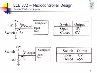
Synchronizing the Interface Chip and the I/O Devices • Brute-force method -- useful when the data timing is unimportant • For input -- Nothing special is done. The microprocessor reads the interface chip and the interface chip returns the voltage levels on the input port pins to the microprocessor. • For output -- Nothing special is done. The interface chip places the data that it received from the microprocessor directly on the output port pins. • The strobe method -- a strobe signal used to indicate that data are stable on I/O port pins • For input -- The interface chip latches the data into its data register using the strobe signal. • For output -- The interface chip places the data on port pins that it received from the microprocessor and asserts the strobe signal. The output device latches the data using the strobe signal. • The handshake method -- used when timing is crucial • Two handshake signals used to synchronize the data transfer. One signal, call it H1, is asserted by the interface chip. The other signal, call it H2, is asserted by the I/O device. • Two handshake modes available • Pulse mode and interlocked mode
Input Handshake Protocol • Step 1. The interface chip asserts (or pulses) H1 to indicate its intention to input data. • Step 2. The input device puts data on the data port pins and also asserts (or pulses) the handshake signal H2. • Step 3. The interface chip latches the data and de-asserts H1. After some delay, the input device also de-asserts H2.
Output Handshake Protocol • Step 1. The interface chip places data on the port pins and asserts (or pulses) H1 to indicate that it has valid data to be output. • Step 2. The output device latches the data and asserts (or pulses) H2 to acknowledge the receipt of data. • Step 3. The interface chip de-asserts H1 following the assertion of H2. The output device then de-asserts H2.
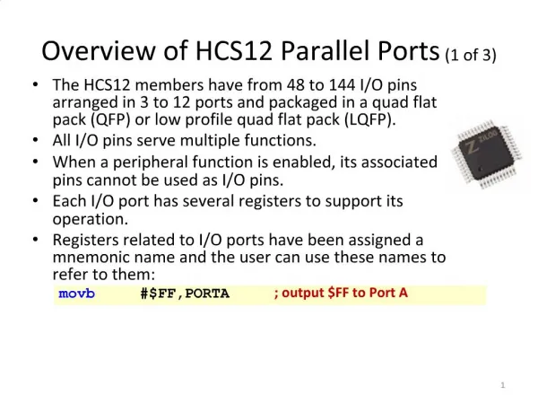
Overview of HCS12 Parallel Ports (1 of 3) • The HCS12 members have from 48 to 144 I/O pins arranged in 3 to 12 ports and packaged in a quad flat pack (QFP) or low profile quad flat pack (LQFP). • All I/O pins serve multiple functions. • When a peripheral function is enabled, its associated pins cannot be used as I/O pins. • Each I/O port has several registers to support its operation. • Registers related to I/O ports have been assigned a mnemonic name and the user can use these names to refer to them: movb #$FF,PTA ; output $FF to Port A
Overview of HCS12 Parallel Ports (2 of 3) • All I/O ports (except PAD0 and PAD1) have an associated data direction register and a data register. • The name of the data direction register is formed by adding the letters “DDR” as the prefix to the port name. For example, DDRA, DDRB, and DDRT. • To configure a pin for output, write a ‘1’ to the associated bit in the data direction register. • To configure a pin for input, write a ‘0’ to the associated bit in the data direction register. movb #$FF,DDRA ; configure port A for output movb #0,DDRA ; configure port A for input bset DDRA,$81 ; configure Port A pin 7 and 1 for output
Overview of HCS12 Parallel Ports (3 of 3) • The name of port data register is formed by adding letters “PT” as the prefix to the port name. For example, PTA, PTB, PTP, and PTT. • We can also use “PORT” as the prefix to the port name for port A, B, E, and K. • Output a value to a port is done by storing that value to the port data register. movb #$FF,DDRH ; configure Port H for output movb #$37,PTH ; output the hex value 37 to port H • Input a value from an input port is done by loading from the port data register. movb #0,DDRH ; configure Port H for input ldaa PTH ; read data from port H into A • An I/O port may have up to eight associated registers.
Port A and Port B • In expanded mode, Port A carries the time-multiplexed higher address/data signals A15/D15…A8/D8. • In expanded mode, Port B carries the time-multiplexed lower address/data signals A7/D7…A0/D0. • In single chip mode, these two ports are used as general I/O ports.
Port E • Port E pins are used for bus control and interrupt service request signals. • When a Port E pin is not used as control or interrupt signal, it can be used as general I/O pin.
Port E Registers • Port E assignment register (PEAR) • In expanded mode, the PEAR register assigns the function of each port E pin. • MODE register • This register establishes the operation mode and other miscellaneous functions. • Pull-up control register (PUCR) • This register selects the pull-up resistors for the pins associated with the core ports. • Port A, B, E, and K are in the core part. • Reduced drive register (RDRIV) • This register selects reduced drive for the pins associated with the core ports. • This gives reduced power consumption and reduced RFI with a slight increase in transition time. • External bus interface control register (EBICTL) • Only bit 0 is implemented (ESTR). • The ESTR bit enables/disables the E clock stretching.
Port K • Has PTK and DDRK registers • Carries expanded address XADDR14…XADDR19 in expanded mode • On the rising edge of the RESET signal, the value of the PK7 pin is latched into the ROMON bit of the MISC register in expanded mode. If it is 1, the on-chip flash memory is enabled. • ROMON is forced to 1 in single chip mode.
Port T • Has Port T data register (PTT), Port T data direction register (DDRT), Port input register (PTIT), reduced drive register (RDRT), pull device enable register (PERT), and port polarity select register (PPST) • The PTIT register allows the user to read back the status of Port T pins. • The RDRT register can configure the drive strength (current output) of each port pin as either full or reduced load. • The PERT register is used to enable an input Port T pin pull-up or pull-down device. • The PPST register selects whether a pull-down or pull-down device is connected to the pin. • Port T pins are also used as timer input capture/output compare pin.
Port S • Port S pins are used as general I/O, serial communication interface, and serial peripheral interface pins. • Port S has a Port S wired-or mode register (WOMS) in addition to all registers associated with Port T.
Port M • Port M has all the equivalent registers that Port S has and also a module routing register (MODRR). • The MODRR configures the rerouting of CAN0, CAN4, SPI0, SPI1, and SPI2 on defined port pins.
Example 7.1 Give an instruction to configure the MODRR register to achieve the following port routing: • 1. CAN0: use pins PM1 and PM0 • 2. CAN1: use pins PM3 and PM2 • 3. CAN2: use pins PM5 and PM4 • 4. CAN3: use pins PM7 and PM6 • 5. I2C: use PJ7 and PJ6 • 6. SPI0: use pins PS7~PS4 • 7. SPI1: use pins PH3~PH0 • 8. SPI2: use pins PH7~PH4 • Solution: This routing requirement can be achieved by preventing CAN4 from using any port pins and keep the default routing after reset. • The following instruction will satisfy the requirement: • movb #$60,MODRR ; CAN4 must be disabled
Example 7.2 Give an instruction to configure the MODRR register to achieve the following port routing: • 1. CAN0: use pins PM1 and PM0 • 2. CAN1: use pins PM3 and PM2 • 3. CAN2: disabled • 4. CAN3: disabled • 5. I2C: use PJ7 and PJ6 • 6. SPI0: use pins PS7~PS4 • 7. SPI1: use pins PP3~PP0 • 8. SPI2: use pins PH7~PH4 • Solution: This routing requirement can be satisfied by the following instruction: • movb #$40,MODRR ; CAN2~CAN4 must be disabled
Port H, J, and P • These three I/O ports have the same set of registers: • Port I/O register (PTH, PTJ, PTP) • Port Input Register (PTIH, PTIJ, PTIP) • Port Data Direction Register (DDRH, DDRJ, DDRP) • Port Reduced Drive Register (RDRH, RDRJ, RDRP) • Port Pull Device Enable Register (PERH, PERJ, PERP) • Port Polarity Select Register (PPSH, PPSJ, PPSP) • Port Interrupt Enable Register (PIEH, PIEJ, PIEP) • Port Interrupt Flag Register (PIFH, PIFJ, PIFP) • These ports have edge-triggered interrupt capability in the wired-OR fashion. • The SPI function pins can be rerouted to Port H and P. • The interrupt edges can be rising or falling and are programmed through Port Device Enable Register and Port Polarity Select Register. • The Port Interrupt Register allows the user to enable interrupts on these three ports.
Port AD0 and AD1 • Many HCS12 devices have two 8-channel A/D converters (AD0 and AD1). • Device that has only one 8-channel module is referred to as AD. • When A/D functions are disabled, these two ports can be used as general input port. • These two ports do not have data direction registers. • Each module has a Digital Input Enable Register. In order to use an A/D pin as a digital input, one needs to set its associated bit in this register.
Electrical Characteristic Consideration for I/O Interfacing • When interfacing I/O device to the MCU, one needs to consider electrical compatibility issues. • There are two electrical compatibility issues: • Voltage level compatibility • Current drive capability • There are many IC technologies in use. Some are bipolar, whereas others are unipolar (mainly CMOS and BICMOS). • Voltage parameters related to electrical compatibility • Input high voltage (VIH) • Input low voltage (VIL) • Output high voltage (VOH) • Output low voltage (VOL)
For Device X to Drive Device Y Correctly • The output high voltage of device X (VOHX) must be higher than the input high voltage of device Y (VIHY). • The output low voltage of device X (VOLX) must be lower than the input low voltage of device Y (VILY). • The input and output voltage levels of several popular logic families are shown in Table 7.3. • At the same power supply level, the CMOS device has no problem in driving the bipolar and CMOS devices. • Bipolar devices have problem in driving CMOS devices. • HCS12 cannot be driven by bipolar devices. • Bipolar devices have problems driving CMOS devices (including HCS12).
Current Drive Capability • The device that drives other devices must have enough sourcing (supply current) and sinking (absorb current) capability. • Current flows out from the driving device when the driving voltage is high. • Current flows into the driving device when the driving voltage is low. • The driving device must be able to supply (or sink) enough current needed by those devices being driven for proper operation. • If a device cannot source or sink enough current, then using buffer device is a common solution. • The current capabilities of a logic device are determined by the following currents: • Input high current (IIH) • Input low current (IIL) • Output high current (IOH) • Output low current (IOL) • The current capability of several logic chip families are shown in Table 7.4.
1. The IOH of an output pin must be equal to or larger than the total current flowing into all the peripheral pins that are connected to this pin. 2. The IOL of an output pin must be equal to or larger than the total current flowing out from all the peripheral pins that are connected to this pin.
Timing Compatibility • There is no timing problem when driving a peripheral pin that does not contain latches or flip-flops. • When driving a latch or flip-flop device, one needs to make sure that the data set up time (tSU) and data hold time (tHD) are both satisfied. • The data setup time and data hold time requirements are illustrated in Figure 7.28.
Interfacing with LED Devices • Figure 7.29 suggests three methods for interfacing with LEDs. • Circuit (a) and (b) are recommended for LEDs that need only small current to light. • Circuit (c) is recommended for LEDs that need larger current to light.
Example 7.3 Use Port B to drive eight LEDs using the circuit shown in Figure 7.30. Light each LED for half a second in turn and repeat assuming the HCS12 has a 24-MHz E clock. - To turn on one LED at a time for half a second in turn, one should output the value $80, $40, $20, $10, $08,$04,$02, and $01 and stay for half a second in each value.
The assembly program that performs the operation is as follows: #include "C:\miniide\hcs12.inc" org $1500 movb #$FF,DDRB ; configure port B for output bset DDRJ,$02 ; configure PJ1 pin for output bclr PTJ,$02 ; enable LEDs to light forever ldaa #16 ; initialize loop count to 8 ldx #led_tab ; use X as the pointer to LED pattern table led_lp movb 1,x+,PTB ; turn on one LED ldy #5 ; wait for half a second jsr delayby100ms ; " dbne a,led_lp ; reach the end of the table yet? bra forever ; start from beginning led_tab dc.b $80,$40,$20,$10,$08,$04,$02,$01 dc.b $01,$02,$04,$08,$10,$20,$40,$80 #include "C:\miniide\delay.asm" end
The C language version of the program is as follows: #include "c:\egnu091\include\hcs12.h" #include "c:\egnu091\include\delay.c" main (void) { char led_tab[8] = {0x80,0x40,0x20,0x10,0x08,0x04,0x02,0x01, 0x01,0x02,0x04,0x08,0x10,0x20,0x40,0x80}; char i; DDRB = 0xFF; /* configure port B for output */ DDRJ |= 0x02; /* configure PJ1 pin for output (needed for DRAGON12 board only) */ PTJ &= 0xFD; /* enable LEDs to light (needed for DRAGON12 board only)*/ while (1){ for (i = 0; i < 16; i++) { PTB = led_tab[i]; delayby100ms(5); } } return 0; }
Driving a Single Seven-Segment Display • A common cathode seven-segment display is driven by the 74HC244 via resistors. • The output high voltage of the 74HC244 is close to 5V with a 5V power supply. • The segment patterns for 0 to 9 are shown in Table 7.5.
Driving Multiple Seven-Segment Displays • Time multiplexing technique is often used to drive multiple displays in order to save I/O pins. • One parallel port is used to drive the segment pattern and the other port turns on one display at a time. Each display is turned on and then off many times within a second. The persistence of vision make us feel that all displays are turned on simultaneously.
Example 7.4 Write a sequence of instructions to display 4 on the seven-segment display #4 in Figure 7.32. • Solution: To display the digit 4 on the display #4, we need to: • Output the hex value $33 to port B • Set the PK4 pin to 1 • Clear pins PK5 and PK3...P0 to 0 #include <hcs12.inc> four equ $33 ; seven-segment pattern of digit 4 movb #$3F,DDRK ; configure PORT K for output movb #$FF,DDRB ; configure PORT B for output bset PTK,$10 ; turn on seven-segment display #4 bclr PTK,$2F ; turn off seven-segment displays #5, #3…#0 movb #four,PTB ; output the seven-segment pattern to PORTP In C language: DDRK = 0x3F; DDRB = 0xFF; PTK = 0x10; PTB = 0x33;
Example 7.5 Write a program to display 123456 on the six seven-segment displays shown in Figure 7.32. • Solution: Display 123456 on display #5, #4, #3, #2, #1, and #0, respectively. • The values to be output to Port B and Port K to display one digit at a time is shown in Table 7.6. - The program logic is shown in Figure 7.33.
#include "c:\miniide\hcs12.inc" pat_port equ PTB ; Port that drives the segment pattern pat_dir equ DDRB ; direction register of the segment pattern sel_port equ PTK ; Port that selects the digit sel_dir equ DDRK ; data direction register of the digit select port org $1500 movb #$FF,pat_dir ; configure pattern port for output movb #$3F,sel_dir ; configure digit select port for output forever ldx #disp_tab ; use X as the pointer loop movb 1,x+,pat_port ; output digit pattern and move the pointer movb 1,x+,sel_port ; output digit select value and move the pointer ldy #1 ; wait for 1 ms jsr delayby1ms ; “ cpx #disp_tab+12 ; reach the end of the table bne loop bra forever #include "c:\miniide\delay.asm" disp_tab dc.b $30,$20 ; seven-segment display table dc.b $6D,$10 dc.b $79,$08 dc.b $33,$04 dc.b $5B,$02 dc.b $5F,$01 end
#include “c:\egnu091\include\hcs12.h” #include “c:\egnu091\include\delay.c” #define pat_port PTB /* segment pattern port */ #define pat_dir DDRB /* pattern port data direction register */ #define sel_port PTK /* digit select port */ #define sel_dir DDRK /* digit select port direction register */ main (void) { char disp_tab[6][2] = {{0x30,0x20},{0x6D,0x10},{0x79,0x08}, {0x33,0x04},{0x5B,0x02},{0x5F,0x01}}; char i; pat_dir = 0xFF; /* configure pat_port for output */ sel_dir = 0x3F; /* configure sel_port for output */ while (1) { for (i = 0; i < 6; i++) { pat_port = disp_tab[i][0]; /* output the segment pattern */ sel_port = disp_tab[i][1]; /* turn on the display */ delaybyms(1); /* wait for 1 ms */ } } return 0; }
Liquid Crystal Display (LCD) (1 of 2) • The basic construction of an LCD is illustrated in Figure 7.34. • The most common type of LCD allows the light to pass through when activated. • An LCD segment is activated when a low frequency bipolar signal in the range of 30 Hz to 1KHz is applied to it. • LCD can display characters and graphics. • LCDs are often sold in a module with LCDs and controller unit built in. • The Hitachi HD44780 is the most popular LCD controller being used today.