
Infineon
E N D
Presentation Transcript
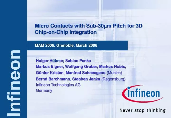
Micro Contacts with Sub-30µm Pitch for 3D Chip-on-Chip Integration MAM 2006, Grenoble, March 2006 Holger Hübner, Sabine Penka Markus Eigner, Wolfgang Gruber, Markus Nobis, Günter Kristen, Manfred Schneegans(Munich) Bernd Barchmann, Stephan Janka(Regensburg) Infineon Technologies AG Germany Infineon
Outline Historical Background Theory and Basics Comparison of BGA vs SOLID Process Flow Cost Comparison with FBGA Experimental Results Reliability Results
Historical Background • Due to the steady increase of information density and shrink of design rules in the silicon • the traditional DIL package had been replaced by surface mount technologies using solder bumps (Ball Grid Arrays – BGA). • and also the first level wire bonds inside the package will be replaced by solder bumps (FBGA Fine Pitch Micro Bumps)
Chip–to–chipinterconnect Chip–to–substr.interconnect Package–to–board interconnects today future? 200µm / pitch 500 µm 120 / 240 60/120 30/60 15/30 Steadily Shrinking Dimensions of BGAs BGA Chip-to Board PbSn Micro bumps Chip-to-Chip Lead free
Problems with Shrinking Dimensions • Decreasing compliance of the solder bump • Increasing growth velocity and influence of intermetallic phases duringsolder reflow - especially for lead free solders • Complicated architecture of the metallization(e.g. Cu – Ni/Au – SnAg – Ni – Cu) • A mix of multiple phases in the solder bump (electro migration driven) • Consumption of diffusion barrier during (high temperature) operation • Risc of erosion of the under-bump metallization
Argumentation for a New Technology Compliance is only given (and needed) for chip-to-board interconnects We focus on chip-to-chip interconnects For chip-to-chip connections bumps must be low-scale and high density If the influence of the intermetallics grows, why not build bumps completely out of intermetallics ? Our new interconnect technology replaces the soft soldering by a soldering process called Solid-Liquid-InterDiffusion (SOLID)
Outline Historical Background Theory and Basics Comparison of BGA vs SOLID Process Flow Cost Comparison with FBGA Experimental Results Reliability Results
MxLy T liquid T Cu6Sn5 () Cu3Sn () 2 solid high melting phase soldering T 1 solid Sn Cu M L Metallurgical Basics of the SOLID Technology Cu - Sn (3µm) - Cu • Sn melts at the soldering temperature (231°C) • Sn and Cu react to Inter Metallic Compounds (IMCs) • The melting point raises by several 100°C to T2 and • The joint solidifies isothermally at the processing temperature
Cu B A C Sn Cu Kinetic of Phase Growth Diffusion paths A - via grain boundaries into the liquid solder B - through the - phases C - via the - phases (less important) Kinetics Initially very rapid Cu-diffusion and growth of -phases via A (convection enhanced material transport within the liquid Sn) At the same time the -phases grow laminar impeding more and more the phase growth (solid state diffusion via C) After Sn is consumed completely, the -phase will be transformed to -phase (solid state diffusion)
Kinetic of Phase Growth * S. BaderMPI für MetallforschungStuttgart, 1990 • A 3 µm gap solidifies within a few ten seconds • The ε-phase needs 15 - 20 min for the transformation of a 3 µm layer
Outline Historical Background Theory and Basics Comparison of BGA vs SOLID Process Flow Cost Comparison with FBGA Experimental Results Reliability Results
Cu Sn Cu Sn Cu3Sn Cu Cu Comparison of Solder Processes BGA - Solder bump SOLID interface diffusion barrier • Very thin solder layer • No barrier • Simple metallurgy • Sn is completely consumed • Solidification isothermally • Large solder volumen • Phase growth is controlled by • diffusion barrier (Ni/Au) and • low temperature budget • Solidification by cooling
SOLID Metallization and solder apply 1st step 2nd step Reflow Pick & place (no flux) 3rd step Pick & place (flux) Soldering 4th step Soldering Comparison of Solder Processes FBGA Metallization and solder apply
Comparison of Processes BGA SOLID Same processing for solder apply, but reflow and soldering in a single stepafter pick & place • Different sizes possible • Different shapes possible • Smaller spacing (only limited by the bonder alignment) • Only two metals involved (barrier free, one IMC) • Thermodynamical stable • Low homologuos temperature • reflow defines shape of the balls before pick & place • All pads must be the same size • All pads must be the same shape • Larger spacing between balls, because balls expand • Complicated metallurgy (barrier, multiple IMCs) • Phase growth not finished • High homologous temperature
200µm / pitch 500 µm 120 / 240 60/120 30/60 15/30 Geometrical Comparison of BGA vs SOLID Soft solder bumps BGA Micro bumps Transition from soft solderto Inter Metallic Compounds (IMC) SOLID contacts 15µm / pitch 30 µm(limited by the bonder alignment accuracy) 7,5/15
SOLID-Face-to-Face Stack Top chipCu and Sn coating Bottom chipCu coating, bond pads No underfill Inter chip vias15 x 15 µm²5 µm vias to LM Redistribution Insulation trenches15 µm Passive areaheat spreader External IOsstandard wire bonds
Benefits of the Planar Metal Interface • One single step for electrical and mechanical contact • Additional wiring layer • Very flat design • Electrical shield / base plane • Excellent heat conduction • Mechanical reinforcement of the point contacts • The top chip does not need an Al layer • No space consumption by testpads(Testpads can be designed within the passive area) • Top chip thinning after soldering • Modular process for multi-tier stacking (Si thru holes)
Outline Historical Background Theory and Basics Comparison of BGA vs SOLID Process Flow Cost Comparison with FBGA Experimental Results Reliability Results
LM M1 IMOX c-Si (Testing)Top wafer thinningSingulationPick, flip and placeSoldering TiW Oxide Cu seed c-Si Resist AlSiCu Sn CuSn Cu Metallization Wafer processes Bond processChip to Wafer Initial stateOpened passivationViasØ 5 µm, Al or Cu SputteringTiW barrier 50nmCu seedlayer 100nm LithoInsulation trenches Plating moduleCu 5µmTop wafer only: Sn 3µmResist stripWet etch seedlayer and barrier
T = 70°C Solidification by cool down T = 25°C T = 25°C Pick & Place 1st Step – Sticking the chips on wafer • Application of a liquid sticking agent by a jet dispenser • The hard contact with the cold wafer • freezes the sticking agent w/o time delay • parallizes the chips (tilt adjustment) • Demands on the sticking agent (bibenzyl): • Melting point 50 - 60°C • High vapour pressure (evaporation in vacuum) • Inert, non corrosive, non hygroscopic • No residues
Soldering 2nd Step – Soldering of the populated wafer • Demands on the soldering process • Evaporation of the sticking agent • Reduction of the Cu- und Sn-surfaces • Complete transformation of Sn to η-phase • No lateral shift of the chips during heating (horizontal placement) • No contamination of the surface (residue-free flux) Process parameters: 1 min @ 260°C; vacuum or inert gas
Alloying 3rd Step (optional) – Final transformation η- into ε-phase • Batch oven • Inert gas Process parameter: 20 min @ 300°C
Outline Historical Background Theory and Basics Comparison of BGA vs SOLID Process Flow Cost Comparison with FBGA Experimental Results Reliability Results
Cost Comparison with FBGA • Wafer metallization is similar to electro plated FBGA • Standard equipment for test, pick & place, soldering and inspection • Only one minor add-on: jet dispenser Cost reduction potential comes from • Thinner metal layers • Additional redistribution layer given „for free“ • No Al-layer in the top chip • No flux cleaning after soldering • No underfill required
Outline Historical Background Theory and Basics Comparison of BGA vs SOLID Process Flow Cost Comparison with FBGA Experimental Results Reliability Results
30 µm Experimental Results • Standard contact with • 15 µm Pitch 30 µm Via to last metal 5 µm Demonstrator for20 µm pitch
Experimental Results • Standars contacts (defined by bonder alignment): 15 x 15 µm², 5 x 5 µm² vias to last metal • 10 µm pads with 20 µm pitch demonstrated • 5 µm crossed lines have successfully been bonded • No influence of particles seen (class 10000 CR) • Thickness of the top chips: 80 µm, typically 125 µm • Shear strength of the bond: >120 N @ 25 mm² chip size • Measured contact resistance: 5 m for a standard contact • Worst case simulation of stray capacities: 34 – 40 fF (w/o and w/ underfill)
R R R C C Contact Circuit line Transit Frequency of a Single Contact Modellumped circuit Contact dimensions 15 x 15 µm² 40 fF (simulation)5 m (measured value) Conductor width 200 nm thickness 350 nm resistance 90 m/ capacitance 250 aF/µm (standard Cu-wire in C9)
Problem: Solder Squeeze Out Redistribution lines are prone to solder sqeeze out Theoretical background (surface tension) allows for exact calculation of design rules Stiched tin volume prohibits solder squeeze-out Wrong design rule (w/o stiching) New design rule(stiched tin lines) X-ray image of a chip stack
Outline Historical Background Theory and Basics Comparison of BGA vs SOLID Process Flow Cost Comparison with FBGA Experimental Results Reliability Results
Corrosion Behaviour of an Uprotected Solder Joint Cu • After 96h @ 121°C, 100% • corrosion of the -phase • -phase is inert • minor Cu-corrosion Reference probe FIB preparation of the chip edge no underfill
Corrosion Free Cavities FIB preparation after 1000 h HTS (85°C, 85%) Top chip thinned by wet etch No corrosion inside the stack cavity. Metallical seal ring Organical sealring (FF2200) protects -phase
Drift of 500 daisy chain dR/R [%] cycles Temperature Cycles (TC) 73 chains of 500 standard contacts (15 x 15 µm², via 5 x 5 µm²) from LM to LM 1000 cycles -65…150°C, 1 h each
Pitch 30µm 5 µm Contact After 500 T-Cycles -65 …150°C Void-free joint Alloying completed by a batch process Only two phases (Cu and Cu3Sn), no barrier No degradation, no re-cristallization Morphology remains unchanged in comparison to the reference probe, beside a growing cross linking during the first cycles
dR/R [%] High Temperature Storage (HTS) 140 chains of 500 standard contacts (15 x 15 µm², via 5 x 5 µm²) from LM to LM Two storage temperatures175°C and 200°C
AC UHAST prestress prestress Humidity Stress Results 15 µm space between solder line and base plane, length 2.5 mm, height 12 µm, with underfiller Leakage current raises due to moisture uptake of the underfiller Resistance remains unchainged
Humidity Stress Results The increase of the leakage current is a geometrical problem, when the insulation gap becomes more and more narrow. This is a technology-independant phenomenon and can also be seen at micro-bumped probes. • It will be a real concern for • small contact distances • for high pin counts • low power devices • Possible counter measures: • Use of underfiller with less moisture uptake • Interface w/o underfiller • Seal ring
Pitch 30µm Self Alignment Despite a not yet optimized design, we succeeded in a self-aligning process with an alignment accuracy of 1 µm (Initial placement 10 µm) Diagonal cut through a contact chain (steps 1 µm each)
Thank you for your attention ! Many thanks to R. Tilgner / IFX for many valuable discussions !