Download
1 / 2
20 likes | 131 Vues
Tuning the properties of silicon nitride Jos é Menéndez , Arizona State University, DMR 0907600.

E N D
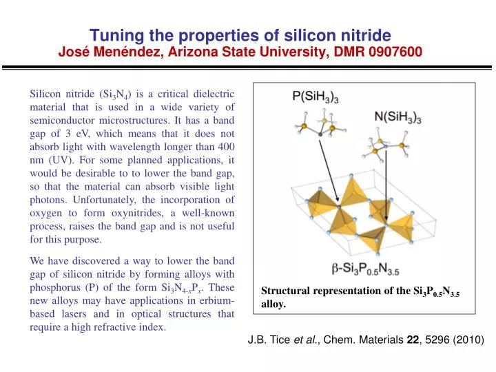
Tuning the properties of silicon nitrideJosé Menéndez, Arizona State University, DMR 0907600 Silicon nitride (Si3N4) is a critical dielectric material that is used in a wide variety of semiconductor microstructures. It has a band gap of 3 eV, which means that it does not absorb light with wavelength longer than 400 nm (UV). For some planned applications, it would be desirable to to lower the band gap, so that the material can absorb visible light photons. Unfortunately, the incorporation of oxygen to form oxynitrides, a well-known process, raises the band gap and is not useful for this purpose. We have discovered a way to lower the band gap of silicon nitride by forming alloys with phosphorus (P) of the form Si3N4-xPx. These new alloys may have applications in erbium-based lasers and in optical structures that require a high refractive index. Structural representation of the Si3P0.5N3.5 alloy. J.B. Tice et al., Chem. Materials 22, 5296 (2010)
Integration of SiGeSn with III-V semiconductorsJosé Menéndez, Arizona State University, DMR 0907600 The ternary GeSiSn alloy semiconductor, developed by us at Arizona State University, is a candidate material for a fourth junction that might increase the performance of commercial three-junction solar cells. Key for this application is the successful growth of III-V materials on GeSiSn and/or the growth of GeSiSn on III-V materials. In collaboration with Emcore, a leading solar cell manufacturer, we have begun to study the growth of GeSiSn on GaAs substrates, and the initial results (see figure) are highly encouraging. Top:XTEM micrograph of Ge0.90Si0.08Sn0.02 grown on bulk GaAs indicating that the layer is flat and devoid of threading defects. Bottom: X-ray (004) diffraction peak demonstrating that the two layers have the same lattice constant.