COPPER Revision and New CPU
260 likes | 385 Vues
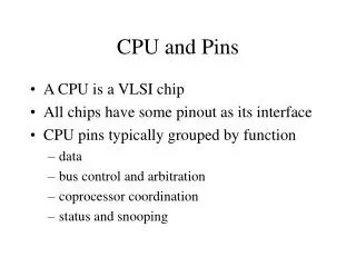
COPPER Revision and New CPU. Part I: Introduction. Readout Electronics Block Diagram. mezzanine (add-on) modules. FIFO. PMC modules. Detector I/F. PMC CPU. PCI bus. local bus. D e t ector I /F. from detector. Network IF. to event builder. Bridge. D e t ector I /F. Trigger Module.

COPPER Revision and New CPU
E N D
Presentation Transcript
Readout Electronics Block Diagram mezzanine(add-on) modules FIFO PMC modules DetectorI/F PMC CPU PCI bus local bus DetectorI/F from detector Network IF to event builder Bridge DetectorI/F Trigger Module DetectorI/F
“COPPER-II” Online CPU module Digitizer module x 4 Add-on modules forthe COPPER RadiSys EPC-6315 • Intel P3 800 MHz • 256 MB memory • Network boot • RedHat Linux 9 VME9U Trigger distributionmodule 100BaseTport x 2 Data link & control link
COPPER-II Performance Review @ 416 bytes/ev/FINESSE 10% Data compr. 40 DigitizerEmulator CPU Required L1 rate 30 DigitizerEmulator CLK/TRGdistribution 20 Accepted L1 rate [kHz] DigitizerEmulator Typical L1 rate 10 Ethernet DigitizerEmulator 0 10 20 30 40 Input L1 rate [kHz] COPPER COPPER-II worksw/ L1 rate >30 kHz RX
2002-2003 Design started. Prototype of the COPPER. 2004 Upgrade to the COPPER-II. Proved to work in severer L1 rate (~30 kHz) than the SuperBelle. 2005 Debug on AMT3 FINESSE. EFC DAQ replaced with the COPPER-II’s (6). Compatibility study btw the COPPER-II and the LeCroy. 2006 Part of CDC DAQ replaced with the COPPER-II’s. More compatibility study. Deadtime study. 2007 Full CDC DAQ replaced with the COPPER-II’s (89). ACC DAQ replaced with the COPPER-II’s (24). 2008 TRG DAQ replaced with the COPPER-II’s (26). Study to replace KLM DAQ is going on. COPPER History in the Belle DAQ Ready to replaceall LeCroy DAQ
Deadtime Reduction by COPPER S.Y.Suzuki Typical data size LeCroy ~29.5 μs By the replacement of theLeCroy with the COPPER-II,DAQ deadtime is reducedby 90%. DAQ deadtime (μs) COPPER-II/AMT3 ~2.8 μs # of hits/TDC
Some parts started to discontinue Need their replacement with up to date parts.Major motivation of the upgrade. • As the technology evolves, price of some parts w/ the higher performance gets much lower:e.g. GbE controller. • Fix some minor inconveniences: e.g. move/change switch positions and shapes for better access. • Delete unused functions so far. COPPER-II “COPPER-3”
The most important rule of the upgrade: The COPPER-3 shall befully compatible with the COPPER-II. • FINESSEs, device drivers, and readout software for the COPPER-II shall be used for the COPPER-3 without any modification at all. COPPER-II COPPER-3
Replace discontinued parts. • Replace discontinuing or out of date parts. • RoHS compliant parts. • Cyclone Cyclone3. • Replace 100Base-T Ethernet controller (82559)w/ GbE controller (82541). • Normalize signal line lengths from the TTRX to each of the 4 FINESSEs. • SCLK, TRG etc. • Move VME signal receivers to much closer position to the VME J0 connector for more stable signal handling. List of Major Upgrade Items
Change reset switch shape more accessible. • Present switch on the front panel is difficult to push. • Move VME base address config. switch to more accessible area. • Remove and simplify unused connectors/patterns originally intended for debug use. • Join 2 FIFOs to 1. Series of two FIFO chips were aligned to form a larger single FIFO so that we could select FIFO size at production. • Change front panel design. List of Major Upgrade Items data data FIFO FIFO FIFO control control
Jun. 2nd: Design work started by the company. Jun. 30th: Design and schematic chart drawing – delayed. Jul.4th: ----- TODAY ----- Jul.18th: FPGA programming. Jul.28th: Pattern layout. Aug.8th: Board production. Aug.29th: Parts assembly. Sep.6th: Board verification. Sep.16th: Document writing. Sep.26th: Delivery to KEK. Dec.31st: End of COPPER-3 study by KEK. COPPER-3 Short Term Schedule
By JFY 2008 • Find out and fix most bugs in the COPPER-3 prototype. Makes COPPER-3 ready for the mass production. • In JFY 2009 • Purchase ~20 COPPER-3. Single-crate system test. • In JFY 2010-2011 • Purchase 200-300 COPPER-3. Build up sBelle DAQ system. • In JFY 2012 • Start sBelle Operation. COPPER-3 Long Term Schedule JFY: Japanese Fiscal Year;from Apr. to Mar.
Major roles related to the data handling: • Readout data from 4 pipeline FIFOs on the COPPER. • Combine an event chunk from each of the FIFOs to form a single event record. • Provide online data monitoring. • Format the event record into the Belle standard. • Transfer the event record to an external readout PC of the COPPER via Ethernet. • Peripheral roles: • Initialize COPPER itself, FINESSE, and TTRX. • Handles run control commands: “RUN-START” / “RUN-STOP” / “FATAL-CONDITION”, etc. • Etc. Roles of the COPPER CPU
EPC-6315 is regarded the standard CPU for the COPPER. • Why EPC-6315? • RadiSys EPC-6315 was the only commercially-available PrPMC (processor PMC) equipped with the Intel CPU when we startedthe COPPER R&D. • Specs: • CPU: Intel PentiumIII 800 MHz • Memory: 256 MB. • The RJ-45 connector for the Ethernet. • RedHat Linux 7.3 or 9,or FedoraCore 1 Linux run on it. • Price: ~1,100 USD / module. RadiSys EPC-6315 Bootable from CF card or from network.
Cons of the EPC-6315 • The EPC-6315 is getting an out-of-date product;its prospect is not very promising. • Chipset (RadiSys 82600)deteriorates the data transfer. • PLX9054 PMC memory • 112 Mbps (w/ DMA) • PLX9054 EPC-6315 memory • 74 Mbps (w/ DMA) • Also, we found that RadiSys was less professional in the customer communication… PMC connector PCI mem. 82600RadiSys The 82600 breaks data transfer every 32 bytes in the burst mode, which is the origin of the bottleneck. It cannot be disabled. EPC-6315 block diagram
GE Fanuc PSL09 – new commercially available PrPMC • CPU: Intel PentiumM 1.4 GHz. • Memory: 256 MB. • Price: ~2,000 USD / module. • 10 COPPER-II’s w/ PSL09 attached hadbeen installed into the DAQ system andhave been tested in the beam operation. • It is observed that they worked quite well.It can be one of the possiblecandidate of the next PrPMC. • I fairy have to say, we haven’t examined if this PrPMC’s chipset would be a bottleneck of the data transfer or not. Other Possibilities of PrPMCs M.Nakao Photo of PSL09 w/heat sink removed
Possibility of a custom CPU • One Japanese company (Advanet) shows a strong interest to develop a new PrPMC. • According to their rough idea… • CPU: Intel Tolapai (code name) 600 MHz equivalent to PentiumM 900MHz. • Memory: 512MB-1GB. • R&D cost: ~100k USD. • Board price: ~1300 USD. • R&D will be finished within this fiscal year. • We keep surveying any kind of better PrPMC. Other Possibilities of PrPMCs Looks a bit costly. We are tonegotiate with them to find outthe possible compromise.
The COPPER-II is to be upgraded to COPPER-3, which has 100% backward compatibility. Within this fiscal year, we will make it ready toward the mass production. • Because of some problems, we are searching for the next PrPMC with which the RadiSys’s EPC-6315 is replaced. Good performance of the GE Fanuc’s PSL09 is proved in the beam operation; the PSL09 is one of the candidates. Beside that, we are searching for possibility of the custom PrPMC. Summary
Readout Electronics Overview from detector • Detector I/F • Signal digitization. • L1 pipeline. Detector I/F • Readout FIFO • Event buffers for asynchronous readout. Readout FIFO Online processor • Online processor • Data size reduction. • Data link management to event builder. to event builder
Design Concept • Modules • Detector I/F • User defined cards for analog part only,minimizing the R&D cost. • Data reduction CPU • Commercially available PMC module,no hardware development cost. • Common platform • DAQ software can be generalized. Low Cost Design
Profile of CPU Usage @ 416 bytes/ev/ADC-module • User time: ~2% • System time: ~20% • Idle time: ~78% = CPU power that is equivalent to P3 ~600MHz is still available • Large idle time fraction indicates the PCI bus works at the full performance. • 416 bytes / ADC-module / ev × 40 kHz × 4 ADC modules= 67 MB/s.
Performance Degradation by Network Use @ 416 bytes/ev/ADC-module CPU user time: ~2% CPU system time: ~20% CPU idle time: ~78% Maximum acceptedtrigger rate: 40 kHz CPU proc.A FIFO Read CPU CPU user time: ~5% CPU system time: ~31% CPU idle time: ~64% Maximum acceptedtrigger rate: 32 kHz proc.A proc.B NetworkTransfer FIFO Read Ethernet 11MB/s RX Still works well.