Chapter 3 General-Purpose Processors: Software
Chapter 3 General-Purpose Processors: Software. Introduction. Processor designed for a variety of computation tasks Low unit cost, in part because manufacturer spreads NRE over large numbers of units Motorola sold half a billion 68HC05 microcontrollers in 1996 alone

Chapter 3 General-Purpose Processors: Software
E N D
Presentation Transcript
Introduction • Processor designed for a variety of computation tasks • Low unit cost, in part because manufacturer spreads NRE over large numbers of units • Motorola sold half a billion 68HC05 microcontrollers in 1996 alone • Carefully designed since higher NRE is acceptable • Can yield good performance, size and power • Low NRE cost, short time-to-market/prototype, high flexibility • User just writes software; no processor design
Processor Control unit Datapath Control /Status Controller ALU PC IR Registers I/O Memory Basic Architecture • Control unit and datapath • N-bit processor • N-bit ALU, registers, buses, memory data interface • 8-bit, 16-bit, 32-bit common • PC size determines address space • Clock cycle impacts processing speed
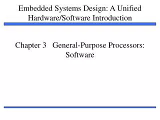
Processor Processor Program memory Data memory Memory (program and data) Harvard Princeton Two Memory Architectures • Princeton • Fewer memory wires • Harvard • Simultaneous program and data memory access
Fast/expensive technology, usually on the same chip Processor Cache Memory Slower/cheaper technology, usually on a different chip Cache Memory • Memory access may be slow • Cache is small but fast memory close to processor • Holds copy of part of memory • Hits and misses
Wash 1 2 3 4 5 6 7 8 1 2 3 4 5 6 7 8 Non-pipelined Pipelined Dry 1 2 3 4 5 6 7 8 1 2 3 4 5 6 7 8 non-pipelined dish cleaning Time pipelined dish cleaning Time Fetch-instr. 1 2 3 4 5 6 7 8 Decode 1 2 3 4 5 6 7 8 Fetch ops. 1 2 3 4 5 6 7 8 Pipelined Execute 1 2 3 4 5 6 7 8 Store res. 1 2 3 4 5 6 7 8 Time pipelined instruction execution Pipelining
Instruction 1 opcode operand1 operand2 Instruction 2 opcode operand1 operand2 Instruction 3 opcode operand1 operand2 Instruction 4 opcode operand1 operand2 ... Instructions Stored In Memory
Addressing mode Register-file contents Memory contents Operand field Immediate Data Register-direct Register address Data Register indirect Register address Memory address Data Direct Memory address Data Indirect Memory address Memory address Data Addressing Modes
A Simple (Trivial) Instruction Set Assembly instruct. First byte Second byte Operation MOV Rn, direct 0000 Rn direct Rn = M(direct) MOV direct, Rn 0001 Rn direct M(direct) = Rn Rm MOV @Rn, Rm 0010 Rn M(Rn) = Rm MOV Rn, #immed. 0011 Rn immediate Rn = immediate ADD Rn, Rm 0100 Rn Rm Rn = Rn + Rm SUB Rn, Rm 0101 Rn Rm Rn = Rn - Rm JZ Rn, relative 0110 Rn relative PC = PC+ relative (only if Rn is 0) opcode operands
C program Equivalent assembly program 0 MOV R0, #0; // total = 0 1 MOV R1, #10; // i = 10 2 MOV R2, #1; // constant 1 int total = 0; for (int i=10; i!=0; i--) total += i; // next instructions... 3 MOV R3, #0; // constant 0 Loop: JZ R1, Next; // Done if i=0 5 ADD R0, R1; // total += i 6 SUB R1, R2; // i-- 7 JZ R3, Loop; // Jump always Next: // next instructions... Sample Programs
LPT Connection Pin I/O Direction Register Address 1 Output 0th bit of register #2 2-9 Output 0th bit of register #2 10,11,12,13,15 Input 6,7,5,4,3th bit of register #1 14,16,17 Output 1,2,3th bit of register #2 Example: parallel port driver • Using assembly language programming we can configure the parallel port to perform digital I/O • write and read to three special registers to accomplish this table provides list of parallel port connector pins and corresponding register location • Example : parallel port monitors the input switch and turns the LED on/off accordingly
Parallel Port Example ; This program consists of a sub-routine that reads ; the state of the input pin, determining the on/off state ; of our switch and asserts the output pin, turning the LED ; on/off accordingly .386 CheckPort proc push ax ; save the content push dx ; save the content mov dx, 3BCh + 1 ; base + 1 for register #1 in al, dx ; read register #1 and al, 10h ; mask out all but bit # 4 cmp al, 0 ; is it 0? jne SwitchOn ; if not, we need to turn the LED on SwitchOff: mov dx, 3BCh + 0 ; base + 0 for register #0 in al, dx ; read the current state of the port and al, f7h ; clear first bit (masking) out dx, al ; write it out to the port jmp Done ; we are done SwitchOn: mov dx, 3BCh + 0 ; base + 0 for register #0 in al, dx ; read the current state of the port or al, 01h ; set first bit (masking) out dx, al ; write it out to the port Done: pop dx ; restore the content pop ax ; restore the content CheckPort endp extern “C” CheckPort(void); // defined in // assembly void main(void) { while( 1 ) { CheckPort(); } }
System Call Invocation • system call is a mechanism for an application to invoke the operation system • operating system • provides software required for servicing hardware interrupts • provides device drivers for driving peripheral devices present on the system DB file_name “out.txt” -- store file name MOV R0, 1324 -- system call “open” id MOV R1, file_name -- address of file-name INT 34 -- cause a system call JZ R0, L1 -- if zero -> error . . . read the file JMP L2 -- bypass error cond. L1: . . . handle the error L2:
Asm. File C File C File Compiler Assembler Binary File Binary File Binary File Linker Debugger Exec. File Profiler Verification Phase Implementation Phase Library Software Development Process
(a) (b) Implementation Phase Implementation Phase Verification Phase Development processor Debugger/ ISS External tools Programmer Verification Phase Emulator Software Design Process
Instruction Set Simulator For A Simple Processor #include <stdio.h> typedef struct { unsigned char first_byte, second_byte; } instruction; instruction program[1024]; //instruction memory unsigned char memory[256]; //data memory void run_program(int num_bytes) { int pc = -1; unsigned char reg[16], fb, sb; while( ++pc < (num_bytes / 2) ) { fb = program[pc].first_byte; sb = program[pc].second_byte; switch( fb >> 4 ) { case 0: reg[fb & 0x0f] = memory[sb]; break; case 1: memory[sb] = reg[fb & 0x0f]; break; case 2: memory[reg[fb & 0x0f]] = reg[sb >> 4]; break; case 3: reg[fb & 0x0f] = sb; break; case 4: reg[fb & 0x0f] += reg[sb >> 4]; break; case 5: reg[fb & 0x0f] -= reg[sb >> 4]; break; case 6: pc += sb; break; default: return –1; } } return 0; } int main(int argc, char *argv[]) { FILE* ifs; If( argc != 2 || (ifs = fopen(argv[1], “rb”) == NULL ) { return –1; } if (run_program(fread(program, sizeof(program) == 0) { print_memory_contents(); return(0); } else return(-1); }
General Purpose Processors Sources: Intel, Motorola, MIPS, ARM, TI, and IBM Website/Datasheet; Embedded Systems Programming, Nov. 1998
Aliases: op IR[15..12] rn IR[11..8] rm IR[7..4] dir IR[7..0] imm IR[7..0] rel IR[7..0] A Simple Microprocessor FSMD FSM operations that replace the FSMD operations after a datapath is created Reset PC=0; PCclr=1; Declarations: bit PC[16], IR[16]; bit M[64k][16], RF[16][16]; IR=M[PC]; PC=PC+1 Fetch MS=10; Irld=1; Mre=1; PCinc=1; Decode from states below Mov1 RF[rn] = M[dir] RFwa=rn; RFwe=1; RFs=01; Ms=01; Mre=1; to Fetch op = 0000 RFr1a=rn; RFr1e=1; Ms=01; Mwe=1; Mov2 M[dir] = RF[rn] 0001 to Fetch RFr1a=rn; RFr1e=1; Ms=10; Mwe=1; Mov3 M[rn] = RF[rm] 0010 to Fetch Mov4 RF[rn]= imm RFwa=rn; RFwe=1; RFs=10; 0011 to Fetch RFwa=rn; RFwe=1; RFs=00; RFr1a=rn; RFr1e=1; RFr2a=rm; RFr2e=1; ALUs=00 Add RF[rn] =RF[rn]+RF[rm] 0100 to Fetch RFwa=rn; RFwe=1; RFs=00; RFr1a=rn; RFr1e=1; RFr2a=rm; RFr2e=1; ALUs=01 Sub RF[rn] = RF[rn]-RF[rm] 0101 to Fetch PCld= ALUz; RFrla=rn; RFrle=1; Jz PC=(RF[rn]=0) ?rel :PC 0110 to Fetch
Datapath 1 Control unit 0 To all input control signals RFs 2x1 mux RFwa Controller (Next-state and control logic; state register) RF (16) RFw RFwe From all output control signals RFr1a RFr1e 16 RFr2a Irld PCld PC IR RFr1 RFr2 PCinc RFr2e ALUs PCclr ALU ALUz 2 1 0 Ms 3x1 mux Mre Mwe Memory D A Architecture Of A Simple Microprocessor • storage devices for each declared variable • register file holds each of the variables • functional units to carry out the FSMD operations • an ALU is used to carry out the required operations • connections added among the components’ ports corresponding to the operations required by the FSM • unique identifiers created for every control signal